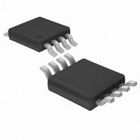
LTC1261LCMS8#TR Linear Technology, LTC1261LCMS8#TR Datasheet - Page 6

LTC1261LCMS8#TR
Manufacturer Part Number
LTC1261LCMS8#TR
Description
IC VOLT INVERT SW CAP ADJ 8MSOP
Manufacturer
Linear Technology
Type
Switched Capacitor (Charge Pump), Invertingr
Datasheet
1.LTC1261LCMS8PBF.pdf
(12 pages)
Specifications of LTC1261LCMS8#TR
Internal Switch(s)
Yes
Synchronous Rectifier
No
Number Of Outputs
1
Voltage - Output
-1.23 ~ -5 V
Current - Output
20mA
Frequency - Switching
650kHz
Voltage - Input
2.7 ~ 5.25 V
Operating Temperature
0°C ~ 70°C
Mounting Type
Surface Mount
Package / Case
8-MSOP, Micro8™, 8-uMAX, 8-uSOP,
Lead Free Status / RoHS Status
Contains lead / RoHS non-compliant
Power - Output
-
Available stocks
Company
Part Number
Manufacturer
Quantity
Price
LTC1261L
APPLICATIONS
The LTC1261L uses an inverting charge pump to generate
a regulated negative output voltage that is either equal to
or less than the supply voltage. The LTC1261L needs only
three external capacitors and is available in the MSOP and
SO-8 packages
THEORY OF OPERATION
A block diagram of the LTC1261L is shown in Figure 1. The
heart of the LTC1261L is the charge pump core shown in
the dashed box. It generates a negative output voltage by
first charging the flying capacitor (C1) between V
ground. It then connects the top of the flying capacitor to
ground, forcing the bottom of the flying capacitor to a
negative voltage. The charge on the flying capacitor is
transferred to the output bypass capacitor, leaving it
charged to the negative output voltage. This process is
driven by the internal 650kHz clock.
Figure 1 shows the charge pump configuration. With the
clock low, C1 is charged to V
rising clock edge, S1 and S3 are open and S2 and S4
6
U
650kHz
CLK
R
S
Q
INFORMATION
U
CC
COMP1
by S1 and S3. At the next
V
REF
+
–
W
= 1.23V
60mV
1.17V
V
U
OUT
Figure 1. Block Diagram
CC
S2
and
V
CC
S1
S3
C1
C1
C1
+
–
+
–
closed. S2 connects C1
the output by S4. The charge in C1 is transferred to C
setting it to a negative voltage.
The output voltage is monitored by COMP1 which com-
pares a divided replica of the output at ADJ (COMP for
fixed output voltage parts) to the internal reference. At the
beginning of a cycle the clock is low, forcing the output of
the AND gate low and charging the flying capacitor. The
next rising clock edge sets the RS latch, setting the charge
pump to transfer charge from the flying capacitor to the
output capacitor. As long as the output is below the set
point, COMP1 stays low, the latch stays set and the charge
pump runs at the full 50% duty cycle of the clock gated
through the AND gate. As the output approaches the set
voltage, COMP1 will trip whenever the divided signal
exceeds the internal 1.23V reference relative to OUT. This
resets the RS latch and truncates the clock pulses, reduc-
ing the amount of charge transferred to the output capaci-
tor and regulating the output voltage. If the output exceeds
the set point, COMP1 stays high, inhibiting the RS latch
and disabling the charge pump.
COMP2
S4
R2
R1
ADJ (COMP)
OUT
REG
+
to ground, C1
+
INTERNALLY
CONNECTED FOR
FIXED OUTPUT
VOLTAGE PARTS
C
OUT
1261L F01
–
is connected to
OUT
,


