LTC1682CMS8-3.3#TRPBF Linear Technology, LTC1682CMS8-3.3#TRPBF Datasheet
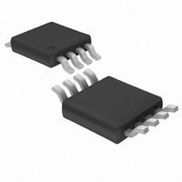
IC MULTI CONFIG 3.3V 90MA 8MSOP

LTC1682CMS8-3.3#TRPBF

Manufacturer Part Number
LTC1682CMS8-3.3#TRPBF
Description
IC MULTI CONFIG 3.3V 90MA 8MSOP
Manufacturer
Linear Technology
Type
Step-Up (Boost), Switched Capacitor (Charge Pump), Doublerr
Datasheet

Specifications of LTC1682CMS8-3.3#TRPBF

Internal Switch(s)
Yes
Synchronous Rectifier
No
Number Of Outputs
1
Voltage - Output
3.3V
Current - Output
90mA
Frequency - Switching
550kHz
Voltage - Input
1.8 ~ 4.4 V
Operating Temperature
0°C ~ 70°C
Mounting Type
Surface Mount
Package / Case
8-MSOP, Micro8™, 8-uMAX, 8-uSOP,
Lead Free Status / RoHS Status
Lead free / RoHS Compliant
Power - Output
-

Available stocks

Company
Part Number
Manufacturer
Quantity
Price
Company:
Part Number:
LTC1682CMS8-3.3#TRPBFLTC1682CMS8-3.3
Manufacturer:
LT
Quantity:
10 000
Company:
Part Number:
LTC1682CMS8-3.3#TRPBFLTC1682CMS8-3.3
Manufacturer:
LT/凌特
Quantity:
20 000
Company:
Part Number:
LTC1682CMS8-3.3#TRPBFLTC1682CMS8-3.3#PBF
Manufacturer:
LINEAR/凌特
Quantity:
20 000
Company:
Part Number:
LTC1682CMS8-3.3#TRPBF
Manufacturer:
AD
Quantity:
2 945
Company:
Part Number:
LTC1682CMS8-3.3#TRPBF
Manufacturer:
LT/凌特
Quantity:
20 000
FEATURES
TYPICAL APPLICATIO
APPLICATIO S
2.5V TO
4.4V
Low Output Noise: 60 V
Adjustable or Fixed Boosted Output
Adjustable Output Voltage Range: 2.5V to 5.5V
Fixed Output Voltages: 3.3V, 5V
Wide Input Voltage Range: 1.8V to 4.4V
Uses Small Ceramic Capacitors
No Inductors Required
Output Current up to 50mA
550kHz Switching Frequency
Low Operating Current: 150 A
Low Shutdown Current: 1 A
Internal Thermal Shutdown and Current Limiting
Available in 8-Pin MSOP and SO Packages
VCO Power Supplies in Cellular Phones
2-Way Pagers
Wireless PCMCIA Cards
Portable Medical Instruments
Low Power Data Acquisition
Remote Transmitters
V
IN
0.22 F
4.7 F
4.7 F
4.2V VCO Power Supply, V
8
7
6
5
U
CPO
C
V
C
IN
+
LTC1682
SHDN
V
RMS
GND
OUT
FB
SHUTDOWN
1
2
3
4
(100kHz BW)
U
15k
36k
4.2V
4.7 F
IN
1 F
= 2.5V to 4.4V
1k
1000pF
1000pF
B
M
MQE001-902
MURATA
VCO
1000pF
P
C
Doubler Charge Pumps with
LTC1682/LTC1682-3.3/LTC1682-5
DESCRIPTIO
The LTC
pumps with an internal low noise, low dropout (LDO) linear
regulator. These parts are designed to provide a low noise
boosted supply voltage for powering noise sensitive devices
such as high frequency VCOs in wireless applications.
An internal doubler charge pump converts a 1.8V to 4.4V
input to a boosted output, while the internal LDO regulator
converts the boosted voltage to a low noise regulated output.
The adjustable version allows the user to set V
resistors connected to FB. The regulator is capable of supply-
ing up to 50mA of output current. Shutdown reduces the
supply current to < 5 A, removes the load from V
disabling the regulator and discharges V
through a 100 switch.
The LTC1682 LDO regulator is stable with only 2 F on the
output. Small ceramic capacitors can be used, reducing PC
board area.
The LTC1682/LTC1682-3.3/LTC1682-5 are short-circuit and
over temperature protected. The parts are available in 8-pin
MSOP and SO packages.
Low Noise Linear Regulator
, LTC and LT are registered trademarks of Linear Technology Corporation.
100k
f
902MHz
OUT
®
1682 TA01
4.7 F
1682/LTC1682-3.3/LTC1682-5 are doubler charge
V
C
AMPLITUDE
10dB/DIV
U
CENTER = 902MHz
SPAN = 100kHz
SWP = 10 sec
Open-Loop Close-In Phase Noise
RES BW = 1kHz
VBW = 30Hz
REF = 0dBm
OUT
OUT
via external
to ground
1682 TA02
IN
1
by

Related parts for LTC1682CMS8-3.3#TRPBF

LTC1682CMS8-3.3#TRPBF Summary of contents

Page 1

... The LTC1682 LDO regulator is stable with only the output. Small ceramic capacitors can be used, reducing PC board area. The LTC1682/LTC1682-3.3/LTC1682-5 are short-circuit and over temperature protected. The parts are available in 8-pin MSOP and SO packages. , LTC and LT are registered trademarks of Linear Technology Corporation. = 2.5V to 4.4V IN 4.2V f OUT ...

Page 2

... Storage Temperature Range ................. – 150 C IN Lead Temperature (Soldering, 10 sec).................. 300 C Maximum Junction Temperature .......................... 125 ORDER PART NUMBER LTC1682CMS8 1 V LTC1682CMS8-3.3 OUT SHDN 2 LTC1682CMS8-5 3 FILT/FB* LTC1682IMS8 GND 4 LTC1682IMS8-3.3 LTC1682IMS8-5 8-LEAD PLASTIC SO MS8 PART MARKING *PIN3 = FILT FOR LTC1682-3.3/LTC1682 FOR LTC1682 LTER LTHM T ...

Page 3

ELECTRICAL CHARACTERISTICS range, otherwise specifications are SHDN = V A PARAMETER CONDITIONS CPO (Charge Pump Output 1.8V Output Resistance 4.4V Dropout Voltage ...

Page 4

LTC1682/LTC1682-3.3/LTC1682 TYPICAL PERFOR A CE CHARACTERISTICS CPO Output Resistance 0. 10mA OUT 1.5 2.0 2.5 3.0 3.5 4.0 ...

Page 5

W U TYPICAL PERFOR A CE CHARACTERISTICS V Voltage vs Temperature OUT 5.030 5.020 I = 10mA OUT 5.010 5.000 4.990 LTC1682-5 3.340 3.330 3.320 LTC1682-3.3 3.310 3.300 3.290 1.240 1.238 LTC1682 1.236 1.234 –50 –25 ...

Page 6

LTC1682/LTC1682-3.3/LTC1682-5 W BLOCK DIAGRA 4.7 F POWER- SHDN 2 ON RESET SD REGEN ENB V REF – CHARGE PUMP AND SLEW CONTROL ENB CLK1 550kHz REG ...

Page 7

W BLOCK DIAGRA 4.7 F POWER- SHDN 2 ON RESET REGEN ENB FILT 3 200k 1nF V REF LTC1682/LTC1682-3.3/LTC1682 – CHARGE PUMP AND SLEW CONTROL ENB CLK1 ...

Page 8

LTC1682/LTC1682-3.3/LTC1682 APPLICATIONS INFORMATION Operation The LTC1682 uses a switched-capacitor charge pump to generate a CPO voltage of approximately 2(V powers an internal low dropout linear regulator that sup- plies a regulated output Internal comparators are ...

Page 9

U U APPLICATIONS INFORMATION The following formula can be used to find the maximum output voltage that may be programmed for a given minimum input voltage and output current load (2)(V ) – (I OUT(MAX) IN(MIN) OUT with ...

Page 10

LTC1682/LTC1682-3.3/LTC1682 APPLICATIONS INFORMATION Power-On Reset Upon initial power-up, a power-on reset circuit ensures that the internal functions are correctly initialized when power is applied. Once V reaches approximately 1V, the IN power-on reset circuit will enable the part ...

Page 11

U TYPICAL APPLICATION C3 4 3.3V C4 4.7 F PACKAGE DESCRIPTION 0.007 0 – 6 TYP (0.18) 0.021 0.006 (0.53 0.015) * DIMENSION DOES NOT INCLUDE MOLD FLASH, PROTRUSIONS OR GATE BURRS. MOLD FLASH, PROTRUSIONS OR GATE ...

Page 12

... GND C 5V LOW NOISE C2 VCO 4.7 F 1682 ta04 C FILT 1nF COMMENTS Generates 5V Varactor Drive from 3V Supply Short Circuit/Thermal Protected CC Micropower; Good Transient Response Ultralow Power: Typical Operating Output Noise CC RMS 128235fs, sn128235 LT/TP 0799 4K • PRINTED IN USA LINEAR TECHNOLOGY CORPORATION 1999 ...

Related keywords