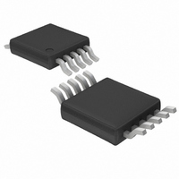
LTC1773EMS#TR Linear Technology, LTC1773EMS#TR Datasheet - Page 6

LTC1773EMS#TR
Manufacturer Part Number
LTC1773EMS#TR
Description
IC CTRLR DC/DC SYNC STPDN 10MSOP
Manufacturer
Linear Technology
Type
Step-Down (Buck)r
Datasheet
1.LTC1773EMS.pdf
(20 pages)
Specifications of LTC1773EMS#TR
Internal Switch(s)
No
Synchronous Rectifier
Yes
Number Of Outputs
1
Voltage - Output
0.8 ~ 8.5 V
Current - Output
6A
Frequency - Switching
550kHz
Voltage - Input
2.65 ~ 8.5 V
Operating Temperature
-40°C ~ 85°C
Mounting Type
Surface Mount
Package / Case
10-MSOP, Micro10™, 10-uMAX, 10-uSOP
Lead Free Status / RoHS Status
Contains lead / RoHS non-compliant
Power - Output
-
Available stocks
Company
Part Number
Manufacturer
Quantity
Price
OPERATIO
LTC1773
Main Control Loop
The LTC1773 uses a constant frequency, current mode
step- down architecture to drive an external pair of comple-
mentary power MOSFETs. During normal operation, the
external top P-channel power MOSFET turns on each cycle
when the oscillator sets the RS latch, and turns off when
the current comparator I
peak inductor current at which I
is controlled by the voltage on the I
output of error amplifier EA. The V
Pin Functions section, allows EA to receive an output
feedback voltage from an external resistive divider. When
the load current increases, it causes a slight decrease in
the feedback voltage relative to the 0.8V reference, which
in turn causes the I
inductor current matches the new load current. While the
top P-channel MOSFET is off, the bottom N-channel
MOSFET is turned on until either the inductor current
starts to reverse, as indicated by the current reversal
comparator I
The main control loop is shut down by pulling the RUN/SS
pin low. Releasing RUN/SS allows an internal 1.5µA
current source to charge the external soft-start capacitor
C
enabled with the internal buffered I
approximately 5% of its maximum value. As C
ues to charge, the internal buffered I
leased allowing normal operation to resume.
An overvoltage comparator, 0V, guards against transient
overshoots (>7.5%) as well as other more serious condi-
tions that may overvoltage the output. In this case, the top
MOSFET is turned off and the bottom MOSFET is turned on
until the overvoltage condition is cleared.
Burst Mode Operation
The LTC1773 is capable of Burst Mode operation in which
the external power MOSFETs operate intermittently based
on load demand. To enable Burst Mode operation, simply
allow the SYNC/FCB pin to float or connect it to a logic
high. To disable Burst Mode operation and force continu-
ous mode, connect the SYNC/FCB pin to GND. The thresh-
old voltage between Burst Mode operation and forced
continuous mode is 0.8V. This can be used to assist in
6
SS
. When C
RCMP
SS
reaches 0.7V, the main control loop is
U
, or the beginning of the next cycle.
TH
voltage to increase until the average
(Refer to Functional Diagram)
COMP
resets the RS latch. The
COMP
FB
TH
pin, described in the
TH
resets the RS latch
voltage clamped at
TH
pin, which is the
is gradually re-
SS
contin-
secondary winding regulation as described in Auxiliary
Winding Control Using SYNC/FCB Pin in the Applications
Information section.
When the converter operates in Burst Mode operation the
peak current of the inductor is set to approximately a third
of the maximum peak current value during normal opera-
tion even though the voltage at the I
value. The voltage at the I
average current is greater than the load requirement. As
the I
tor trips, causing the internal sleep line to go high and turn
off both power MOSFETs.
The circuit enters sleep mode with both power MOSFETs
turned off. In sleep mode, the internal circuitry is partially
turned off, reducing the quiescent current to about 80µA.
The load current is now being supplied from the output
capacitor. When the output voltage drops, causing I
rise above 0.27V, the internal sleep line goes low, and the
LTC1773 resumes normal operation. The next oscillator
cycle will turn on the external top MOSFET and the switch-
ing cycle repeats.
Short-Circuit Protection
When the output is shorted to ground, the frequency of the
oscillator is reduced to about 55kHz, 1/10 the nominal
frequency. This frequency foldback ensures that the in-
ductor current has more time to decay, thereby preventing
runaway. The oscillator’s frequency will gradually in-
crease to 550kHz after V
Frequency Synchronization
The LTC1773 can be synchronized with an external TTL/
CMOS compatible clock signal. The frequency range of
this signal must be from 585kHz to 750kHz. Do not
synchronize the LTC1773 below 585kHz as this may cause
abnormal operation and an undesired frequency spec-
trum. The top MOSFET turn-on follows the rising edge of
the external source.
When the LTC1773 is clocked by an external source, Burst
Mode operation is disabled; the LTC1773 then operates in
PWM pulse skipping mode preventing current reversal. In
this mode, when the output load is very low, current
comparator I
TH
voltage drops below 0.22V, the BURST compara-
COMP
remains tripped for more than one cycle
FB
TH
pin drops when the inductor’s
rises above 0.4V.
TH
pin indicates a lower
TH
1773fb
to


