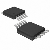
LTC1773EMS#TR Linear Technology, LTC1773EMS#TR Datasheet - Page 9

LTC1773EMS#TR
Manufacturer Part Number
LTC1773EMS#TR
Description
IC CTRLR DC/DC SYNC STPDN 10MSOP
Manufacturer
Linear Technology
Type
Step-Down (Buck)r
Datasheet
1.LTC1773EMS.pdf
(20 pages)
Specifications of LTC1773EMS#TR
Internal Switch(s)
No
Synchronous Rectifier
Yes
Number Of Outputs
1
Voltage - Output
0.8 ~ 8.5 V
Current - Output
6A
Frequency - Switching
550kHz
Voltage - Input
2.65 ~ 8.5 V
Operating Temperature
-40°C ~ 85°C
Mounting Type
Surface Mount
Package / Case
10-MSOP, Micro10™, 10-uMAX, 10-uSOP
Lead Free Status / RoHS Status
Contains lead / RoHS non-compliant
Power - Output
-
Available stocks
Company
Part Number
Manufacturer
Quantity
Price
APPLICATIONS
where δ is the temperature dependency of R
is a constant inversely related to the gate drive current.
Both MOSFETs have I
equation includes an additional term for transition losses,
which are highest at high input voltages. The synchronous
MOSFET losses are greatest at high input voltage or during
a short-circuit when the duty cycle in this switch is nearly
100%.
The term (1 + δ) is generally given for a MOSFET in the
form of a normalized R
δ = 0.005/°C can be used as an approximation for low
voltage MOSFETs. C
characteristics. The constant K = 1.7 can be used to
estimate the contributions of the two terms in the main
switch dissipation equation.
Typical gate charge for the selected P-channel MOSFET
should be less than 30nC (at 4.5V
delay should be less than 150ns. However, due to differ-
ences in test and specification methods of various MOSFET
manufacturers, the P-channel MOSFET ultimately should
be evaluated in the actual LTC1773 application circuit to
ensure proper operation.
A Schottky diode can be placed in parallel with the syn-
chronous MOSFET to improve efficiency. It conducts
during the dead-time between the conduction of the two
power MOSFETs. This prevents the body diode of the
bottom MOSFET from turning on and storing charge
during the dead-time, which could cost as much as 1% in
efficiency. A 1A Schottky is generally a good size for 5A to
8A regulators due to the relatively small average current.
Larger diodes result in additional transition losses due to
their larger junction capacitance. The diode may be omit-
ted if the efficiency loss can be tolerated.
In continuous mode, the source current of the top MOSFET
is a square wave of duty cycle V
voltage transients, a low ESR input capacitor sized for the
maximum RMS current must be used. The maximum
C
IN
P
SYNC
Selection
=
V
IN
–
V
IN
V
OUT
U
RSS
2
R losses while the topside P-channel
(
DS(ON)
is usually specified in the MOSFET
I
INFORMATION
MAX
U
)
2
vs temperature curve, but
(
OUT
1 δ
+
GS
W
/V
)
) while the turn-off
IN
R
. To prevent large
DS ON
( )
DS(ON)
U
and K
RMS capacitor current is given by:
This formula has a maximum at V
I
commonly used for design because even significant de-
viations do not offer much relief. Note that capacitor
manufacturer’s ripple current ratings are often based on
2000 hours of life. This makes it advisable to further derate
the capacitor, or choose a capacitor rated at a higher
temperature than required. Several capacitors may also be
paralleled to meet size or height requirements in the
design. Always consult the manufacturer if there is any
question.
C
The selection of C
series resistance (ESR). Typically, once the ESR require-
ment is satisfied the capacitance is adequate for filtering.
The output ripple (∆V
where f = operating frequency, C
and ∆I
is highest at maximum input voltage since ∆I
with input voltage. With ∆I
for 2/3 of the ripple due to ESR, the output ripple will be
less than 50mV at max V
The first condition relates to the ripple current into the ESR
of the output capacitance while the second term guaran-
tees that the output voltage does not significantly dis-
charge during the operating frequency period due to ripple
current. The choice of using smaller output capacitance
increases the ripple voltage due to the discharging term
but can be compensated for by using capacitors of very
low ESR to maintain the ripple voltage at or below 50mV.
RMS
OUT
C
C
C required I
∆
OUT
OUT
IN
V
Selection
= I
OUT
L
= ripple current in the inductor. The output ripple
> 1/(8fR
required ESR < 2 R
OUT
≅
/2. This simple worst-case condition is
∆
I ESR
L
⎛
⎜
⎝
SENSE
RMS
OUT
OUT
)
is driven by the required effective
+
≅
8
I
IN
) is determined by:
MAX
fC
L
assuming:
SENSE
1
OUT
= 0.4I
[
V
OUT
OUT
⎞
⎟
⎠
OUT(MAX)
= output capacitance
(
IN
V
IN
V
LTC1773
IN
= 2V
–
V
and allowing
OUT
OUT
L
increases
)
, where
]
1 2
1773fb
9


