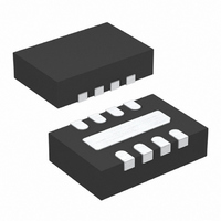
LT3470AEDDB#TRMPBF Linear Technology, LT3470AEDDB#TRMPBF Datasheet - Page 13

LT3470AEDDB#TRMPBF
Manufacturer Part Number
LT3470AEDDB#TRMPBF
Description
IC BUCK ADJ .25A 8DFN
Manufacturer
Linear Technology
Type
Step-Down (Buck)r
Datasheet
1.LT3470AEDDBTRMPBF.pdf
(20 pages)
Specifications of LT3470AEDDB#TRMPBF
Internal Switch(s)
Yes
Synchronous Rectifier
No
Number Of Outputs
1
Voltage - Output
1.25 ~ 16 V
Current - Output
250mA
Voltage - Input
4 ~ 40 V
Operating Temperature
-40°C ~ 85°C
Mounting Type
Surface Mount
Package / Case
8-DFN
Lead Free Status / RoHS Status
Lead free / RoHS Compliant
Power - Output
-
Frequency - Switching
-
Available stocks
Company
Part Number
Manufacturer
Quantity
Price
APPLICATIONS INFORMATION
PCB Layout
For proper operation and minimum EMI, care must be
taken during printed circuit board layout. Note that large,
switched currents flow in the power switch, the internal
catch diode and the input capacitor. The loop formed by
these components should be as small as possible. Further-
more, the system ground should be tied to the regulator
ground in only one place; this prevents the switched cur-
rent from injecting noise into the system ground. These
components, along with the inductor and output capacitor,
should be placed on the same side of the circuit board,
and their connections should be made on that layer. Place
a local, unbroken ground plane below these components,
and tie this ground plane to system ground at one location,
Figure 5. A Good PCB Layout Ensures Proper, Low EMI Operation
V
OUT
ideally at the ground terminal of the output capacitor C2.
Additionally, the SW and BOOST nodes should be kept as
small as possible. Unshielded inductors can induce noise
in the feedback path resulting in instability and increased
output ripple. To avoid this problem, use vias to route the
V
(as shown in Figure 5). Finally, keep the FB node as small
as possible so that the ground pin and ground traces will
shield it from the SW and BOOST nodes. Figure 5 shows
component placement with trace, ground plane and via
locations. Include vias near the GND pin, or pad, of the
LT3470A to help remove heat from the LT3470A to the
ground plane.
OUT
trace under the ground plane to the feedback divider
3470a F05
SHDN
V
GND
IN
LT3470A
13
3470afb


