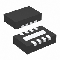
LT3470AEDDB#TRMPBF Linear Technology, LT3470AEDDB#TRMPBF Datasheet - Page 7

LT3470AEDDB#TRMPBF
Manufacturer Part Number
LT3470AEDDB#TRMPBF
Description
IC BUCK ADJ .25A 8DFN
Manufacturer
Linear Technology
Type
Step-Down (Buck)r
Datasheet
1.LT3470AEDDBTRMPBF.pdf
(20 pages)
Specifications of LT3470AEDDB#TRMPBF
Internal Switch(s)
Yes
Synchronous Rectifier
No
Number Of Outputs
1
Voltage - Output
1.25 ~ 16 V
Current - Output
250mA
Voltage - Input
4 ~ 40 V
Operating Temperature
-40°C ~ 85°C
Mounting Type
Surface Mount
Package / Case
8-DFN
Lead Free Status / RoHS Status
Lead free / RoHS Compliant
Power - Output
-
Frequency - Switching
-
Available stocks
Company
Part Number
Manufacturer
Quantity
Price
PIN FUNCTIONS
SHDN (Pin 8): The SHDN pin is used to put the LT3470A in
shutdown mode. Tie to ground to shut down the LT3470A.
Apply 2V or more for normal operation. If the shutdown
feature is not used, tie this pin to the V
NC (Pin 7): This pin can be left floating, connected to V
or tied to GND.
V
internal regulator and to the internal power switch. This
pin must be locally bypassed.
GND (Pin 5): Tie the GND pin to a local ground plane
below the LT3470A and the circuit components. Return
the feedback divider to this pin.
SW (Pin 4): The SW pin is the output of the internal power
switch. Connect this pin to the inductor, catch diode and
boost capacitor.
BLOCK DIAGRAM
IN
(Pin 6): The V
V
IN
C1
IN
pin supplies current to the LT3470A’s
V
NC
SHDN
IN
ONE SHOT
500ns
1.25V
V
REF
R2
FB
R1
BURST MODE
IN
R
S
DETECT
pin.
g
m
ENABLE
Qʹ
Q
+
–
IN
,
BOOST (Pin 3): The BOOST pin is used to provide a drive
voltage, which is higher than the input voltage, to the
internal bipolar NPN power switch.
BIAS (Pin 2): The BIAS pin connects to the internal boost
Schottky diode and to the internal regulator. Tie to V
when V
the BIAS pin will supply current to the internal regulator.
FB (Pin 1): The LT3470A regulates its feedback pin to
1.25V. Connect the feedback resistor divider tap to this
pin. Set the output voltage according to V
+ R1/R2) or R1 = R2 (V
Exposed Pad (Pin 9): Ground. Must be soldered to PCB.
–
+
OUT
> 2.5V or to V
GND
BOOST
BIAS
SW
OUT
IN
/1.25 – 1).
otherwise. When V
C3
L1
C2
3470a BD
LT3470A
OUT
V
OUT
= 1.25V (1
BIAS
3470afb
> 3V
7
OUT


