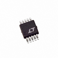
LTC3824HMSE#TRPBF Linear Technology, LTC3824HMSE#TRPBF Datasheet - Page 10

LTC3824HMSE#TRPBF
Manufacturer Part Number
LTC3824HMSE#TRPBF
Description
IC CTRLR STP-DWN HV 10-MSOP
Manufacturer
Linear Technology
Type
Step-Down (Buck)r
Datasheet
1.LTC3824EMSETRPBF.pdf
(14 pages)
Specifications of LTC3824HMSE#TRPBF
Internal Switch(s)
No
Synchronous Rectifier
No
Number Of Outputs
1
Voltage - Output
0.8 ~ 36 V
Current - Output
2A
Frequency - Switching
200kHz ~ 400kHz
Voltage - Input
4 ~ 60 V
Operating Temperature
-40°C ~ 150°C
Mounting Type
Surface Mount
Package / Case
10-MSOP Exposed Pad, 10-HMSOP, 10-eMSOP
Lead Free Status / RoHS Status
Lead free / RoHS Compliant
Power - Output
-
Available stocks
Company
Part Number
Manufacturer
Quantity
Price
applicaTions inForMaTion
LTC3824
on the P-channel switch duty cycle. At high input voltages
the diode conducts most of the time. As V
V
The worst condition for the diode is when the output is
shorted to ground. Under this condition the diode must
safely handle the maximum current at close to 100% of
the time. Therefore, the diode must be carefully chosen
to meet the worst case voltage and current requirements.
Under normal conditions, the average current conducted
by the diode is:
A fast switching Schottky diode must be used to optimize
efficiency.
C
A low ESR input capacitor, C
RMS P-channel switch current is required to prevent large
input voltage transients. The maximum RMS capacitor
current is given by:
This formula has a maximum at V
I
for design because even significant deviations do not offer
much relief. Note that ripple current ratings from capacitor
manufacturers are often based on only 2000 hours of life
which makes it advisable to further derate the capacitor,
or choose a capacitor rated at a higher temperature than
required. Several capacitors may also be paralleled to meet
size or height requirements in the design.
The selection of C
resistance (ESR) that is required to minimize voltage ripple
and load step transients as well as the amount of bulk
capacitance that is necessary to ensure that the control
loop is stable.
The output ripple, ∆V
10
OUT
OUT
IN
I
I
ΔV
D
RMS
and C
/2. This simple worst-case condition is commonly used
= I
the diode conducts only a small fraction of the time.
OUT
OUT
=I
OUT
≤ ΔI
OUT(MAX)
• (1 – D)
Selection
L
ESR+
OUT
V
V
is determined by the effective series
OUT
OUT
IN
8fC
, is determined by:
1
OUT
V
V
IN
OUT
IN
, sized for the maximum
IN
– 1
= 2V
OUT
IN
, where I
approaches
RMS
=
The output ripple is highest at maximum input voltage
since ∆I
placed in parallel may be needed to meet the ESR and
RMS current handling requirements. Dry tantalum, special
polymer, aluminum electrolytic and ceramic capacitors are
all available in surface mount packages. Special polymer
capacitors offer very low ESR but have lower capacitance
density than other types. Tantalum capacitors have the
highest capacitance density but it is important to only
use types that have been surge tested for use in switching
power supplies. Aluminum electrolytic capacitors have
significantly higher ESR, but can be used in cost-sensitive
applications provided that consideration is given to ripple
current ratings and long-term reliability. Ceramic capaci-
tors have excellent low ESR characteristics but can have
a high voltage coefficient and audible noise.
Efficiency Considerations
The efficiency of a switching regulator is equal to the output
power divided by the input power. Percentage efficiency
can be expressed as:
where L1, L2, L3...are the individual loss components as a
percentage of the input power. It is often useful to analyze
individual losses to determine what is limiting the efficiency
and which change would produce the most improvement.
Although all dissipative elements in the circuit produce
losses, the following are the main sources:
1. The supply current into V
% Efficiency = 100%–(L1 + L2 + L3 +......)
of the DC supply current and the MOSFET driver and
control currents. The DC supply current into the V
is typically about 1mA. The driver current results from
switching the gate capacitance of the power MOSFET;
this current is typically much larger than the DC current.
Each time the MOSFET is switched on and off, a packet
of gate charge Q
V
The resulting dQ/dt is a current that must be supplied
to the capacitor by the internal regulator.
CC
I
P
Q
IC
throughout the external bypass capacitor, C
L
= 1mA + f • Q
= V
increases with input voltage. Multiple capacitors
IN
• I
Q
G
G
is transferred from the CAP pin to
CC
. The V
CC
current is the sum
CC
3824fg
CAP
pin
.


