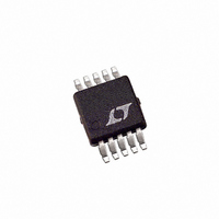
LTC3824HMSE#TRPBF Linear Technology, LTC3824HMSE#TRPBF Datasheet - Page 6

LTC3824HMSE#TRPBF
Manufacturer Part Number
LTC3824HMSE#TRPBF
Description
IC CTRLR STP-DWN HV 10-MSOP
Manufacturer
Linear Technology
Type
Step-Down (Buck)r
Datasheet
1.LTC3824EMSETRPBF.pdf
(14 pages)
Specifications of LTC3824HMSE#TRPBF
Internal Switch(s)
No
Synchronous Rectifier
No
Number Of Outputs
1
Voltage - Output
0.8 ~ 36 V
Current - Output
2A
Frequency - Switching
200kHz ~ 400kHz
Voltage - Input
4 ~ 60 V
Operating Temperature
-40°C ~ 150°C
Mounting Type
Surface Mount
Package / Case
10-MSOP Exposed Pad, 10-HMSOP, 10-eMSOP
Lead Free Status / RoHS Status
Lead free / RoHS Compliant
Power - Output
-
Available stocks
Company
Part Number
Manufacturer
Quantity
Price
LTC3824
pin FuncTions
GND (Pin 1): Chip Ground Pin.
SYNC/MODE (Pin 2): Synchronization Input and Burst
Mode Operation Enable/Disable. If this pin is left open
or pulled higher than 2V, Burst Mode operation will be
enabled at light load and the typical threshold of entering
Burst Mode operation is one third of current limit. If this
pin is grounded or the synchronization pulse is present
with a frequency greater than 20kHz then Burst Mode
operation is disabled and the LTC3824 goes into pulse
skipping at light loads. To synchronize the LTC3824, the
duty cycle of the synchronizing pulse can range from 10%
to 70% and the synchronizing frequency has to be higher
than the programmed frequency.
R
LTC3824 switching frequency.
V
and the control signal of the current mode PWM control
loop. Switching starts at 0.7V, and higher V
to higher inductor current. When V
the LTC3824 goes into micropower shutdown.
6
C
SET
(Pin 4): The Output of the voltage error amplifier gm
(Pin 3): A resistor from R
SET
C
is pulled below 25mV,
to ground sets the
C
corresponds
V
divider to this pin sets the output voltage. When V
less than 0.5V, the switching frequency will fold back to
50kHz to reduce the minimum on-cycle.
SS (Pin 6): Soft-Start Pin. A capacitor on this pin sets
the output ramp-up rate. The typical time for SS to
reach the programmed level is (C • 0.8V)/5µA.
SENSE (Pin 7): Current Sense Input Pin. A sense re-
sistor, R
100mV/R
V
ing is required.
GATE (Pin 9): Gate Drive for The External P-channel
MOSFET. Typical peak drive current is 2.5A and the drive
voltage is clamped to 8V when V
CAP (Pin 10): A Low ESR Capacitor of at Least 0.1µF is
required from this pin to V
tor for biasing the gate driver circuitry.
GND (Exposed Pad Pin 11): Ground. Must be soldered
to PCB with expanded metal trace for rated thermal per-
formance.
FB
CC
(Pin 8): Chip Power Supply. Power supply bypass-
(Pin 5): Error Amplifier Inverting Input. A resistor
S
, from V
S
.
IN
to SENSE sets the current limit to
CC
to bypass the internal regula-
CC
is higher than 9V.
FB
3824fg
is


