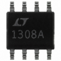
LT1308ACS8 Linear Technology, LT1308ACS8 Datasheet - Page 4

LT1308ACS8
Manufacturer Part Number
LT1308ACS8
Description
IC DC/DC CONV SINGLE CELL 8-SOIC
Manufacturer
Linear Technology
Type
Step-Up (Boost)r
Datasheet
1.LT1308ACS8PBF.pdf
(20 pages)
Specifications of LT1308ACS8
Internal Switch(s)
Yes
Synchronous Rectifier
No
Number Of Outputs
1
Voltage - Output
5V
Current - Output
1A
Frequency - Switching
600kHz
Voltage - Input
1 ~ 10 V
Operating Temperature
0°C ~ 70°C
Mounting Type
Surface Mount
Package / Case
8-SOIC (3.9mm Width)
Lead Free Status / RoHS Status
Contains lead / RoHS non-compliant
Power - Output
-
Available stocks
Company
Part Number
Manufacturer
Quantity
Price
Part Number:
LT1308ACS8
Manufacturer:
LINEAR/凌特
Quantity:
20 000
Part Number:
LT1308ACS8#PBF
Manufacturer:
LINEAR/凌特
Quantity:
20 000
Part Number:
LT1308ACS8#TRPBF
Manufacturer:
LINEAR/凌特
Quantity:
20 000
LT1308A/LT1308B
ELECTRICAL CHARACTERISTICS
range, otherwise specifi cations are at T
Note 1: Stresses beyond those listed under Absolute Maximum Ratings
may cause permanent damage to the device. Exposure to any Absolute
Maximum Rating condition for extended periods may affect device
reliability and lifetime.
Note 2: The LT1308ACS8, LT1308ACF , LT1308BCS8 and LT1308BCF are
designed, characterized and expected to meet the industrial temperature
limits, but are not tested at –40°C and 85°C. I grade devices are
guaranteed over the –40°C to 85°C operating temperature range.
Note 3: Bias current fl ows into FB pin.
TYPICAL PERFORMANCE CHARACTERISTICS
SYMBOL
f
4
OSC
95
90
85
80
75
70
65
60
55
50
1
LT1308B
3.3V Output Effi ciency
PARAMETER
Switching Frequency
Maximum Duty Cycle
Switch Current Limit
Switch V
Burst Mode Operation Switch Current Limit
(LT1308A)
Shutdown Pin Current
LBI Threshold Voltage
LBO Output Low
LBO Leakage Current
LBI Input Bias Current (Note 5)
Low-Battery Detector Gain
Switch Leakage Current
LOAD CURRENT (mA)
V
10
IN
= 1.8V
CESAT
V
IN
= 1.2V
100
V
IN
= 2.5V
1308A/B G01
A
= 25°C. Industrial Grade –40°C to 85°C. V
1000
95
90
85
80
75
70
65
60
55
50
1
LT1308A
3.3V Output Effi ciency
CONDITIONS
Duty Cycle = 30% (Note 4)
I
I
V
V
V
V
I
V
V
V
SW
SW
SINK
IN
SHDN
SHDN
SHDN
LBI
LBI
SW
The
V
= 2.5V, Circuit of Figure 1
= 2A (25°C, – 40°C), V
= 2A (85°C), V
IN
= 250mV, V
= 150mV
= 5V
= 50μA
= 1.1V
= 6V
= 0V
= 1.8V
LOAD CURRENT (mA)
l
10
denotes the specifi cations which apply over the full operating temperature
Note 4: Switch current limit guaranteed by design and/or correlation to
static tests. Duty cycle affects current limit due to ramp generator (see
Block Diagram).
Note 5: Bias current fl ows out of LBI pin.
Note 6: Connect the four GND pins (Pins 4–7) together at the device.
Similarly, connect the three SW pins (Pins 8–10) together and the two V
pins (Pins 11, 12) together at the device.
LBO
V
IN
IN
V
= 1.2V
= 5V
IN
= 1.5V
100
= 2.5V
IN
IN
= 1.2V, V
= 1.5V
1308A/B G02
1000
SHDN
= V
l
l
l
l
l
l
l
l
95
90
85
80
75
70
65
60
55
50
IN
, unless otherwise noted.
1
LT1308A
5V Output Effi ciency
MIN
500
196
193
V
82
2
IN
= 3.6V
LOAD CURRENT (mA)
10
3000
0.01
0.01
0.01
TYP
600
290
330
400
200
200
0.1
90
20
33
3
2
V
IN
= 1.5V
100
MAX
0.25
750
350
400
204
207
100
4.5
0.1
0.1
35
10
5
V
V
IN
IN
= 4.2V
1308A/B G03
= 2.5V
1000
1308abfb
UNITS
kHz
V/V
mV
mV
mA
mV
mV
IN
μA
μA
μA
μA
nA
μA
%
A
V


