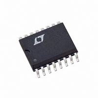
LT1376CS Linear Technology, LT1376CS Datasheet - Page 14

LT1376CS
Manufacturer Part Number
LT1376CS
Description
IC SW REG 1.5A ADJ STP-DWN16SOIC
Manufacturer
Linear Technology
Type
Step-Down (Buck)r
Datasheet
1.LT1376CS8PBF.pdf
(28 pages)
Specifications of LT1376CS
Internal Switch(s)
Yes
Synchronous Rectifier
No
Number Of Outputs
1
Voltage - Output
2.42 ~ 21.5 V
Current - Output
1.5A
Frequency - Switching
500kHz
Voltage - Input
5 ~ 25 V
Operating Temperature
0°C ~ 125°C
Mounting Type
Surface Mount
Package / Case
16-SOIC (3.9mm Width)
Lead Free Status / RoHS Status
Contains lead / RoHS non-compliant
Power - Output
-
Available stocks
Company
Part Number
Manufacturer
Quantity
Price
Part Number:
LT1376CS
Manufacturer:
LINEAR/凌特
Quantity:
20 000
Company:
Part Number:
LT1376CS-5
Manufacturer:
AGERE
Quantity:
1 314
Part Number:
LT1376CS8
Manufacturer:
LINEAR/凌特
Quantity:
20 000
Part Number:
LT1376CS8#PBF
Manufacturer:
LINEAR/凌特
Quantity:
20 000
Company:
Part Number:
LT1376CS8#TR
Manufacturer:
LINEAR
Quantity:
7 388
Company:
Part Number:
LT1376CS8#TRPBF
Manufacturer:
LINEAR
Quantity:
10 119
Part Number:
LT1376CS8#TRPBF
Manufacturer:
LINEAR/凌特
Quantity:
20 000
Part Number:
LT1376CS8-5
Manufacturer:
LINEAR/凌特
Quantity:
20 000
Company:
Part Number:
LT1376CS8-5#TR
Manufacturer:
LT
Quantity:
41
LT1375/LT1376
APPLICATIONS
regulator input voltage. Average forward current in normal
operation can be calculated from:
This formula will not yield values higher than 1A with
maximum load current of 1.25A unless the ratio of input
to output voltage exceeds 5:1. The only reason to consider
a larger diode is the worst-case condition of a high input
voltage and overloaded (not shorted) output. Under short-
circuit conditions, foldback current limit will reduce diode
current to less than 1A, but if the output is overloaded and
does not fall to less than 1/3 of nominal output voltage,
foldback will not take effect. With the overloaded condi-
tion, output current will increase to a typical value of 1.8A,
determined by peak switch current limit of 2A. With
V
This is safe for short periods of time, but it would be
prudent to check with the diode manufacturer if continu-
ous operation under these conditions must be tolerated.
BOOST PIN CONSIDERATIONS
For most applications, the boost components are a 0.1µF
capacitor and a 1N914 or 1N4148 diode. The anode is
connected to the regulated output voltage and this gener-
ates a voltage across the boost capacitor nearly identical
to the regulated output. In certain applications, the anode
may instead be connected to the unregulated input volt-
age. This could be necessary if the regulated output
voltage is very low (< 3V) or if the input voltage is less than
6V. Efficiency is not affected by the capacitor value, but the
capacitor should have an ESR of less than 2Ω to ensure
that it can be recharged fully under the worst-case condi-
tion of minimum input voltage. Almost any type of film or
ceramic capacitor will work fine.
WARNING! Peak voltage on the BOOST pin is the sum of
unregulated input voltage plus the voltage across the
boost capacitor. This normally means that peak BOOST
14
IN
I
I
D AVG
D AVG
= 15V, V
( )
( )
=
=
I
1 8 15 4
OUT
OUT
.
(
(
= 4V (5V overloaded) and I
15
V
IN
V
U
−
IN
−
)
V
OUT
=
INFORMATION
U
1 32
.
)
A
W
OUT
U
= 1.8A:
pin voltage is equal to input voltage plus output voltage,
but when the boost diode is connected to the regulator
input, peak BOOST pin voltage is equal to twice the input
voltage. Be sure that BOOST pin voltage does not exceed
its maximum rating .
For nearly all applications, a 0.1uF boost capacitor works
just fine, but for the curious, more details are provided
here. The size of the boost capacitor is determined by
switch drive current requirements. During switch on time,
drain current on the capacitor is approximately 10mA +
I
drain of 27mA. Capacitor ripple voltage is equal to the
product of on time and drain current divided by capacitor
value; ∆V = t
to less than 0.5V (a slightly arbitrary number) at the worst-
case condition of t
0.1µF. Boost capacitor ripple voltage is not a critical
parameter, but if the minimum voltage across the capaci-
tor drops to less than 3V, the power switch may not
saturate fully and efficiency will drop. An approximate
formula for absolute minimum capacitor value is:
f = Switching frequency
V
V
This formula can yield capacitor values substantially less
than 0.1µF, but it should be used with caution since it does
not take into account secondary factors such as capacitor
series resistance, capacitance shift with temperature and
output overload.
SHUTDOWN FUNCTION AND UNDERVOLTAGE
LOCKOUT
Figure 4 shows how to add undervoltage lockout (UVLO)
to the LT1376. Typically, UVLO is used in situations where
the input supply is current limited , or has a relatively high
source resistance. A switching regulator draws constant
power from the source, so source current increases as
source voltage drops. This looks like a negative resistance
load to the source and can cause the source to current limit
OUT
OUT
IN
C
= Minimum input voltage
/ 75. At peak load current of 1.25A, this gives a total
MIN
= Regulated output voltage
=
(
10
ON
mA I
• 27mA/C. To keep capacitor ripple voltage
+
( )
ON
f V
OUT
(
= 1.8µs, the capacitor needs to be
OUT
/
75
−
)(
3
V
V
OUT
)
/
V
IN
)
13756fd


