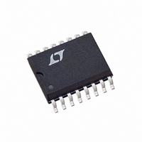
LT1376CS Linear Technology, LT1376CS Datasheet - Page 9

LT1376CS
Manufacturer Part Number
LT1376CS
Description
IC SW REG 1.5A ADJ STP-DWN16SOIC
Manufacturer
Linear Technology
Type
Step-Down (Buck)r
Datasheet
1.LT1376CS8PBF.pdf
(28 pages)
Specifications of LT1376CS
Internal Switch(s)
Yes
Synchronous Rectifier
No
Number Of Outputs
1
Voltage - Output
2.42 ~ 21.5 V
Current - Output
1.5A
Frequency - Switching
500kHz
Voltage - Input
5 ~ 25 V
Operating Temperature
0°C ~ 125°C
Mounting Type
Surface Mount
Package / Case
16-SOIC (3.9mm Width)
Lead Free Status / RoHS Status
Contains lead / RoHS non-compliant
Power - Output
-
Available stocks
Company
Part Number
Manufacturer
Quantity
Price
Part Number:
LT1376CS
Manufacturer:
LINEAR/凌特
Quantity:
20 000
Company:
Part Number:
LT1376CS-5
Manufacturer:
AGERE
Quantity:
1 314
Part Number:
LT1376CS8
Manufacturer:
LINEAR/凌特
Quantity:
20 000
Part Number:
LT1376CS8#PBF
Manufacturer:
LINEAR/凌特
Quantity:
20 000
Company:
Part Number:
LT1376CS8#TR
Manufacturer:
LINEAR
Quantity:
7 388
Company:
Part Number:
LT1376CS8#TRPBF
Manufacturer:
LINEAR
Quantity:
10 119
Part Number:
LT1376CS8#TRPBF
Manufacturer:
LINEAR/凌特
Quantity:
20 000
Part Number:
LT1376CS8-5
Manufacturer:
LINEAR/凌特
Quantity:
20 000
Company:
Part Number:
LT1376CS8-5#TR
Manufacturer:
LT
Quantity:
41
APPLICATIONS
Please read the following if divider resistors are increased
above the suggested values.
Table 1
More Than Just Voltage Feedback
The feedback (FB) pin is used for more than just output
voltage sensing. It also reduces switching frequency and
current limit when output voltage is very low (see the
Frequency Foldback graph in Typical Performance Char-
acteristics). This is done to control power dissipation in
both the IC and in the external diode and inductor during
short-circuit conditions. A shorted output requires the
switching regulator to operate at very low duty cycles, and
the average current through the diode and inductor is
VOLTAGE
OUTPUT
R
(V)
3.3
1
10
12
15
3
5
6
8
=
R V
2
(
OUT
2 42
(k
4.99
4.99
4.99
4.99
4.99
4.99
4.99
4.99
R2
.
Ω
−
)
U
2 42
.
V
LT1375/LT1376
(NEAREST 1%)
C
)
INFORMATION
U
(k
1.21
1.82
5.36
7.32
11.5
15.8
19.6
26.1
R1
Ω
Q2
)
GND
AMPLIFIER
W
R5
5k
ERROR
DUE TO DISCREET 1%
% ERROR AT OUTPUT
Figure 2. Frequency and Current Limit Foldback
RESISTOR STEPS
TO FREQUENCY
SHIFTING
+
–
+ 0.23
+ 0.08
+ 0.39
– 0.04
+ 0.83
– 0.62
+ 0.52
– 0.5
1.6V
U
2.4V
Q1
R3
1k
equal to the short-circuit current limit of the switch (typi-
cally 2A for the LT1376, folding back to less than 1A).
Minimum switch on time limitations would prevent the
switcher from attaining a sufficiently low duty cycle if
switching frequency were maintained at 500kHz, so fre-
quency is reduced by about 5:1 when the feedback pin
voltage drops below 1V (see Frequency Foldback graph).
This does not affect operation with normal load condi-
tions; one simply sees a gear shift in switching frequency
during start-up as the output voltage rises.
In addition to lower switching frequency, the LT1376 also
operates at lower switch current limit when the feedback
pin voltage drops below 1.7V. Q2 in Figure 2 performs this
function by clamping the V
normal 2.3V upper clamp level. This foldback current limit
greatly reduces power dissipation in the IC, diode and
inductor during short-circuit conditions. Again, it is nearly
transparent to the user under normal load conditions. The
only loads which may be affected are current source loads
which maintain full load current with output voltage less
than 50% of final value. In these rare situations the
Feedback pin can be clamped above 1.5V with an external
diode to defeat foldback current limit. Caution: clamping
the feedback pin means that frequency shifting will also be
defeated, so a combination of high input voltage and dead
shorted output may cause the LT1376 to lose control of
current limit.
The internal circuitry which forces reduced switching
frequency also causes current to flow out of the feedback
R4
1k
V
SW
FB
R1
R2
5k
+
C
pin to a voltage less than its
1375/76 F02
OUTPUT
5V
LT1375/LT1376
13756fd
9


