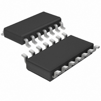
LTC1265CS Linear Technology, LTC1265CS Datasheet - Page 5

LTC1265CS
Manufacturer Part Number
LTC1265CS
Description
IC DC/DC CONV STEP-DOWN 14-SOIC
Manufacturer
Linear Technology
Type
Step-Down (Buck)r
Datasheet
1.LTC1265CSPBF.pdf
(16 pages)
Specifications of LTC1265CS
Internal Switch(s)
Yes
Synchronous Rectifier
No
Number Of Outputs
1
Voltage - Output
1.25 ~ 13 V
Current - Output
1.2A
Frequency - Switching
700kHz
Voltage - Input
3.5 ~ 12 V
Operating Temperature
0°C ~ 70°C
Mounting Type
Surface Mount
Package / Case
14-SOIC (3.9mm Width), 14-SOL
Lead Free Status / RoHS Status
Contains lead / RoHS non-compliant
Power - Output
-
Available stocks
Company
Part Number
Manufacturer
Quantity
Price
Company:
Part Number:
LTC1265CS
Manufacturer:
Linear Technology
Quantity:
135
Company:
Part Number:
LTC1265CS
Manufacturer:
TOKO
Quantity:
1 000
Part Number:
LTC1265CS
Manufacturer:
LT/凌特
Quantity:
20 000
Company:
Part Number:
LTC1265CS#PBF
Manufacturer:
LT
Quantity:
1 493
Part Number:
LTC1265CS-3.3
Manufacturer:
LINEAR/凌特
Quantity:
20 000
Part Number:
LTC1265CS-3.3#TRPBF
Manufacturer:
LINEAR/凌特
Quantity:
20 000
Part Number:
LTC1265CS-5.0
Manufacturer:
LINEAR/凌特
Quantity:
20 000
FU CTIO AL DIAGRA
OPERATIO
The LTC1265 uses a constant off-time architecture to
switch its internal P-channel power MOSFET. The off time
is set by an external timing capacitor at C
operating frequency is then determined by the off time and
the difference between V
The output voltage is set by an internal resistive divider
(LTC1265-3.3 and LTC1265-5) connected to SENSE
(Pin 7) or an external divider returned to V
LTC1265). A voltage comparator V, and a gain block G,
compare the divided output voltage with a reference
voltage of 1.25V.
To optimize efficiency, the LTC1265 automatically switches
between continuous and Burst Mode operation. The volt-
age comparator is the primary control element when the
device is in Burst Mode operation, while the gain block
controls the output voltage in continuous mode.
When the load is heavy, the LTC1265 is in continuous
operation. During the switch ON time, current comparator
C monitors the voltage between Pins 7 and 8 connected
across an external shunt in series with the inductor. When
U
SLEEP
S
U
+
–
U
5
C
T
V
(Refer to Functional Diagram)
TH2
IN
and V
V
TH1
OUT
W
Q
–
+
.
T
R
S
OFF-TIME
CONTROL
(Pin 9 connection shown for LTC1265-3.3 and LTC1265-5; change create LTC1265)
T
12
FB
(Pin 5). The
1, 13
PGND
(Pin 9 for
PWR V
2
SENSE
V
FB
V
IN
14
IN
–
–
SW
C
LTC1265/LTC1265-3.3/LTC1265-5
+
–
11
3
the voltage across the shunt reaches the comparator’s
threshold value, its output signal will change state, setting
the flip flop and turning the internal P-channel MOSFET off.
The timing capacitor connected to Pin 5 is now allowed to
discharge at a rate determined by the off-time controller.
When the voltage on the timing capacitor has discharged
past V
the switch to turn on. Also, the timing capacitor is re-
charged. The inductor current will again ramp up until the
current comparator C trips. The cycle then repeats.
When the load current increases, the output voltage de-
creases slightly. This causes the output of the gain stage
(Pin 6) to increase the current comparator threshold, thus
tracking the load current.
When the load is relatively light, the LTC1265 automati-
cally goes into Burst Mode operation. The current loop is
interrupted when the output voltage exceeds the desired
regulated value. The hysteretic voltage comparator V trips
when V
off the switch and causing the capacitor to discharge. This
I
TH
LB
SGND
25mV TO 150mV
6
0UT
V
TH1
OUT
–
+
, comparator T trips, sets the flip flop and causes
13k
A3
is above the desired output voltage, shutting
+
–
SENSE
G
8
+
–
+
REFERENCE
4
LB
V
OS
IN
SHDN
SENSE
10
7
100k
–
9
1265 FD
V
ADJUSTABLE
VERSION
5pF
FB
5


