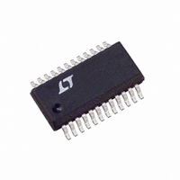
LTC3713EG Linear Technology, LTC3713EG Datasheet

LTC3713EG
Specifications of LTC3713EG
Available stocks
Related parts for LTC3713EG
LTC3713EG Summary of contents
Page 1
... Fault protection is provided by internal foldback current limit- ing, an output overvoltage comparator and an optional short-circuit shutdown timer. , LTC and LT are registered trademarks of Linear Technology Corporation trademark of Linear Technology Corporation. SENSE ...
Page 2
... RNG CC FB1 0.84V RNG FB1 0.84V RNG FB1 V = INTV , V = 0.84V RNG CC FB1 RUN/SS Pin Rising RUN/SS Pin Falling U W ORDER PART TOP VIEW NUMBER 1 BOOST LTC3713EG 3 SW1 SENSE 21 – 5 SENSE 20 6 PGND1 INTV IN1 IN2 11 14 PGND2 12 13 ...
Page 3
... SHDN Note 1: Absolute Maximum Ratings are those values beyond which the life of a device may be impaired. Note calculated from the ambient temperature T J dissipation P as follows: D LTC3713EG • 130 C/ Note 3: The LTC3713 is tested in a feedback loop that adjusts V The denotes specifications which apply over the full operating = 25 C ...
Page 4
LTC3713 W U TYPICAL PERFOR A CE CHARACTERISTICS Transient Response V OUT 100mV/DIV I L 5A/DIV 50 s/DIV 3713 G01 LOAD STEP 3. 1.25V OUT FCB = 0V FIGURE 1 CIRCUIT Boost ...
Page 5
W U TYPICAL PERFOR A CE CHARACTERISTICS Load Regulation 0 –0.1 –0.2 –0.3 –0.4 –0.5 –0.6 FIGURE 1 CIRCUIT –0 LOAD CURRENT (A) 3713 G11 On-Time vs V Voltage ...
Page 6
LTC3713 W U TYPICAL PERFOR A CE CHARACTERISTICS Feedback Reference Voltage vs Temperature 0.82 0.81 0.80 0.79 0.78 –50 – 100 125 TEMPERATURE ( C) 3713 G20 Current Sense Threshold Voltage 300 2V ...
Page 7
CTIO S RUN/SS (Pin 1): Run Control and Soft-Start Input. A capacitor to ground at this pin sets the ramp time to full output current (approximately 3s/ F) and the time delay for overcurrent latchoff ...
Page 8
LTC3713 CTIO AL DIAGRA 0.7V 2.4V V VON t = (10pF ION 20k + I CMP – 1.4V V RNG 4 0.7V 3 240k ...
Page 9
U OPERATIO Main Control Loop The LTC3713 is a current mode controller for DC/DC step-down converters designed to operate from low input voltages. It incorporates a boost converter with a buck regulator. Buck Regulator Operation In normal operation, the top ...
Page 10
LTC3713 U OPERATIO switch cycle, turning on the switch. When the summation of a signal representing switch current and a ramp gen- erator (introduced to avoid subharmonic oscillations at duty factors greater than 50%) exceeds the V comparator A2 changes ...
Page 11
U U APPLICATIO S I FOR ATIO + SENSE WITHOUT R SENSE + SENSE – SENSE OUT R R OS2 OS1 Figure 2. Sense Voltage Offset range with respect to zero current. This can be accom- ...
Page 12
LTC3713 U U APPLICATIO S I FOR ATIO The resulting power dissipation in the MOSFETs at maxi- mum output current are TOP TOP OUT(MAX) T(TOP OUT(MAX) RSS ...
Page 13
U U APPLICATIO S I FOR ATIO specific application. A good starting point is to feed about 25% of the voltage change at the I TH shown in Figure 4a. Place capacitance on the V filter out the I variations ...
Page 14
LTC3713 U U APPLICATIO S I FOR ATIO Tantalum capacitors have the highest capacitance density but it is important to only use types that have been surge tested for use in switching power supplies. Aluminum electrolytic capacitors have significantly higher ...
Page 15
U U APPLICATIO S I FOR ATIO due to a dropping input voltage for example, then the output will drop out of regulation. The minimum input voltage to avoid dropout is OFF MIN ( ) V V ...
Page 16
LTC3713 U U APPLICATIO S I FOR ATIO be estimated from: C > C • V • R (10 SS OUT OUT SENSE Generally 0 more than sufficient. Overcurrent latchoff operation is not always needed or desired. Load ...
Page 17
U U APPLICATIO S I FOR ATIO loss. For example 0.01 and R DS(ON) loss will range from 10% as the output current varies from 1A to 10A for a 1.5V output. 2. Transition ...
Page 18
LTC3713 U U APPLICATIO S I FOR ATIO 013 . . TOP ...
Page 19
U U APPLICATIO S I FOR ATIO PC Board Layout Checklist When laying out a PC board follow one of the two suggested approaches. The simple PC board layout requires a dedicated ground plane layer. Also, for higher currents, it ...
Page 20
LTC3713 U TYPICAL APPLICATIO 0.1 F 100k PGOOD 680pF C 20k 6 C2 100pF 330k 5. 10k 11 ...
Page 21
U TYPICAL APPLICATIO 100k PGOOD R1 R3 10k MBR0520 R2 LT1738 10k – 10k C1 330pF R F1 1.62k R F3 12.1k One-Half Bus Terminator ...
Page 22
LTC3713 U TYPICAL APPLICATIO S Dual Output 1.25V/10A Buck Converter and 5V to 12V/130mA Boost Converter 0.1 F 100k PGOOD C1 R 680pF C 20k C2 100pF R ON 330k 10k ...
Page 23
... FLASH SHALL NOT EXCEED .254mm (.010") PER SIDE Information furnished by Linear Technology Corporation is believed to be accurate and reliable. However, no responsibility is assumed for its use. Linear Technology Corporation makes no represen- tation that the interconnection of its circuits as described herein will not infringe on existing patent rights. ...
Page 24
... Adjustable SENSE LTC3718 Low V DDR Memory and SSTL Termination Power Supply IN LTC3778 No R Synchronous Step-Down Controller SENSE ThinSOT is a trademark of Linear Technology Corporation. Linear Technology Corporation 24 1630 McCarthy Blvd., Milpitas, CA 95035-7417 (408) 432-1900 FAX: (408) 434-0507 3. Synchronous Boost Converter 0.1 F ...


