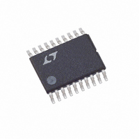
LTC3417AIFE-2#TRPBF Linear Technology, LTC3417AIFE-2#TRPBF Datasheet - Page 12

LTC3417AIFE-2#TRPBF
Manufacturer Part Number
LTC3417AIFE-2#TRPBF
Description
IC BUCK SYNC ADJ 1A/1.5A 20TSSOP
Manufacturer
Linear Technology
Type
Step-Down (Buck)r
Datasheet
1.LTC3417AEDHC-2PBF.pdf
(20 pages)
Specifications of LTC3417AIFE-2#TRPBF
Internal Switch(s)
Yes
Synchronous Rectifier
Yes
Number Of Outputs
2
Voltage - Output
0.8 ~ 5 V
Current - Output
1A, 1.5A
Frequency - Switching
1.5MHz, 0.6MHz ~ 4MHz
Voltage - Input
2.25 ~ 5.5 V
Operating Temperature
-40°C ~ 125°C
Mounting Type
Surface Mount
Package / Case
20-TSSOP Exposed Pad, 20-eTSSOP, 20-HTSSOP
Lead Free Status / RoHS Status
Lead free / RoHS Compliant
Power - Output
-
Available stocks
Company
Part Number
Manufacturer
Quantity
Price
APPLICATIONS INFORMATION
LTC3417A-2
is given to ripple current ratings and long term reliability.
Ceramic capacitors have the lowest ESR and cost but also
have the lowest capacitance density, high voltage and
temperature coeffi cient and exhibit audible piezoelectric
effects. In addition, the high Q of ceramic capacitors along
with trace inductance can lead to signifi cant ringing. Other
capacitor types include the Panasonic specialty polymer
(SP) capacitors.
In most cases, 0.1μF to 1μF of ceramic capacitors should
also be placed close to the LTC3417A-2 in parallel with the
main capacitors for high frequency decoupling.
Ceramic Input and Output Capacitors
Higher value, lower cost ceramic capacitors are now
becoming available in smaller case sizes. Because the
LTC3417 control loop does not depend on the output
capacitor’s ESR for stable operation, ceramic capacitors
can be used freely to achieve very low output ripple and
small circuit size. When choosing the input and output
ceramic capacitors, choose the X5R or X7R dielectric
formulations. These dielectrics have the best temperature
and voltage characteristics of all the ceramics for a given
value and size.
Great care must be taken when using only ceramic input
and output capacitors. When a ceramic capacitor is used
at the input and the power is being supplied through long
wires, such as from a wall adapter, a load step at the output
can induce ringing at the V
couple to the output and be mistaken as loop instability.
At worst, the ringing at the input can be large enough to
damage the part.
Since the ESR of a ceramic capacitor is so low, the input
and output capacitor must fulfi ll a charge storage re-
quirement. During a load step, the output capacitor must
instantaneously supply the current to support the load
until the feedback loop raises the switch current enough
to support the load. The time required for the feedback
12
IN
pin. At best, this ringing can
loop to respond is dependent on the compensation com-
ponents and the output capacitor size. Typically, 3 to 4
cycles are required to respond to a load step, but only in
the fi rst cycle does the output drop linearly. The output
droop, V
droop of the fi rst cycle. Thus, a good place to start is with
the output capacitor size of approximately:
More capacitance may be required depending on the duty
cycle and load step requirements.
In most applications, the input capacitor is merely required
to supply high frequency bypassing, since the impedance
to the supply is very low. A 10μF ceramic capacitor is
usually enough for these conditions.
Setting the Output Voltage
The LTC3417A-2 develops a 0.8V reference voltage between
the feedback pins, V
as shown in Figure 4. The output voltages are set by two
resistive dividers according to the following formulas:
Keeping the current small (<5μA) in these resistors
maximizes effi ciency, but making the current too small
may allow stray capacitance to cause noise problems and
reduce the phase margin of the error amp loop.
To improve the frequency response, a feed-forward capaci-
tor, C
route the V
inductor or the SW line.
C
V
V
OUT1
OUT2
OUT
F
, may also be used. Great care should be taken to
≈ 2.5
DROOP
FB
0.8V 1+
0.8V 1+
node away from noise sources, such as the
f
O
, is usually about 2 to 3 times the linear
• V
ΔI
OUT
DROOP
FB1
R2
R1
R3
R4
and V
FB2
, and the signal ground
3417a2fa


