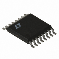
LT1977IFE Linear Technology, LT1977IFE Datasheet - Page 22

LT1977IFE
Manufacturer Part Number
LT1977IFE
Description
IC REG SW 1.5A HV STPDWN 16TSSOP
Manufacturer
Linear Technology
Type
Step-Down (Buck)r
Datasheet
1.LT1977EFEPBF.pdf
(24 pages)
Specifications of LT1977IFE
Internal Switch(s)
Yes
Synchronous Rectifier
No
Number Of Outputs
1
Voltage - Output
1.2 ~ 54 V
Current - Output
1.5A
Frequency - Switching
500kHz
Voltage - Input
3.3 ~ 60 V
Operating Temperature
-40°C ~ 125°C
Mounting Type
Surface Mount
Package / Case
16-TSSOP Exposed Pad, 16-eTSSOP, 16-HTSSOP
Lead Free Status / RoHS Status
Contains lead / RoHS non-compliant
Power - Output
-
Available stocks
Company
Part Number
Manufacturer
Quantity
Price
Company:
Part Number:
LT1977IFE#PBF
Manufacturer:
LT
Quantity:
2 500
Part Number:
LT1977IFE#PBF
Manufacturer:
LINEAR/凌特
Quantity:
20 000
LT1977
APPLICATIO S I FOR ATIO
2. The simultaneous requirements of high V
FREQUENCY COMPENSATION
Before starting on the theoretical analysis of frequency
response the following should be remembered—the worse
the board layout, the more difficult the circuit will be to
stabilize. This is true of almost all high frequency analog
circuits. Read the Layout Considerations section first.
Common layout errors that appear as stability problems
are distant placement of input decoupling capacitor and/or
catch diode and connecting the V
ground track carrying significant switch current. In addi-
tion the theoretical analysis considers only first order non-
ideal component behavior. For these reasons, it is important
that a final stability check is made with production layout
and components.
The LT1977 uses current mode control. This alleviates
many of the phase shift problems associated with the
inductor. The basic regulator loop is shown in Figure 12.
The LT1977 can be considered as two g
amplifier and the power stage.
Figure 13 shows the overall loop response with a 330pF V
capacitor and a typical 100µF tantalum output capacitor.
22
C
R
C
C
power. In questionable cases a prototype supply should
be built and exercised to verify acceptable operation.
high f
switch on time. Cycle skipping and/or Burst Mode be-
havior will result causing an increase in output voltage
ripple while maintaining the correct output voltage.
C
F
OSC
11
LT1977
V
can result in an unacceptably short minimum
CURRENT MODE
POWER STAGE
C
Figure 13. Model for Loop Response
g
m
= 3
Ω
g
U
1.5M
m
= 650µ
ERROR
U
Ω
AMP
+
–
W
1.25V
C
SW
FB
compensation to a
12
m
2
R1
R2
blocks, the error
IN
, low V
1977 F13
U
C
FB
OUT
ESR
C
OUTPUT
OUT
and
C
The response is set by the following terms:
The pole set by C
Unity gain frequency is set by C
Powerstage: DC gain is set by g
Pole set by C
Unity gain set by C
Tantalum output capacitor zero is set by C
ESR
The zero produced by the ESR of the tantalum output ca-
pacitor is very useful in maintaining stability. If better
transient response is required, a zero can be added to the
loop using a resistor (R
capacitor(s). As the value of R
sponse will generally improve but two effects limit its value.
Error amplifier: DC gain is set by g
EA Pole = 1/(2π • 1.5M • 330pF) = 322Hz
EA Unity Gain Frequency = 650µ /(2π • 330pF)
PS DC Gain = 3 • 10 = 30
PS Pole = 1/(2π • 100µF • 10) = 159Hz
PS Unity Gain Freq = 3/(2π • 100µF) = 4.7kHz.
Output Capacitor Zero = 1/(2π • 100µF • 0.1) = 159kHz
EA Gain = 650µ • 1.5M = 975
–50
100
50
0
OUT
10
Figure 14. Overall Loop Response
F
and R
100
and R
OUT
Ω
and g
L
FREQUENCY (Hz)
C
:
L
) in series with a compensation
1k
:
= 313kHz
m
C
V
C
C
R
I
:
LOAD
10k
OUT
OUT
F
C
is increased, transient re-
m
F
/C
= 330pF
C
and g
= 3.3V
= 100µF, 0.1Ω
and R
= 350mA
= NC
100k
m
m
and R
L
1977 F14
:
(assume 10Ω):
1M
OUT
100
135
90
45
0
O
:
and C
1977fa
OUT


