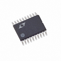
LTC3417AIFE#TRPBF Linear Technology, LTC3417AIFE#TRPBF Datasheet - Page 14

LTC3417AIFE#TRPBF
Manufacturer Part Number
LTC3417AIFE#TRPBF
Description
IC DC/DC CONV DUAL 20TSSOP
Manufacturer
Linear Technology
Type
Step-Down (Buck)r
Datasheet
1.LTC3417AEDHCPBF.pdf
(20 pages)
Specifications of LTC3417AIFE#TRPBF
Internal Switch(s)
Yes
Synchronous Rectifier
Yes
Number Of Outputs
2
Voltage - Output
0.8 ~ 5 V
Current - Output
1A, 1.5A
Frequency - Switching
1.5MHz, 0.6MHz ~ 4MHz
Voltage - Input
2.25 ~ 5.5 V
Operating Temperature
-40°C ~ 85°C
Mounting Type
Surface Mount
Package / Case
20-TSSOP Exposed Pad, 20-eTSSOP, 20-HTSSOP
Lead Free Status / RoHS Status
Lead free / RoHS Compliant
Power - Output
-
Available stocks
Company
Part Number
Manufacturer
Quantity
Price
APPLICATIONS INFORMATION
LTC3417A
determined. The output capacitors need to be selected
because of various types and values determine the loop
feedback factor gain and phase. An output current pulse
of 20% to 100% of full load current having a rise time
of 1μs to 10μs will produce output voltage and I
waveforms that will give a sense of overall loop stability
without breaking the feedback loop.
Switching regulators take several cycles to respond to a
step in load current. When a load step occurs, V
mediately shifts by an amount equal to ΔI
where ESR
ΔI
ing a feedback error signal used by the regulator to return
V
V
indicate a stability problem.
The initial output voltage step may not be within the band-
width of the feedback loop, so the standard second order
overshoot/DC ratio cannot be used to determine phase
margin. The gain of the loop increases with R
bandwidth of the loop increases with decreasing C
R
the zero frequency will be kept the same, thereby keeping
the phase the same in the most critical frequency range
of the feedback loop. In addition, feedforward capacitors,
C1 and C2, can be added to improve the high frequency
response, as shown in Figure 4. Capacitor C1 provides
phase lead by creating a high frequency zero with R1
which improves the phase margin for the 1.5A SW1 chan-
nel. Capacitor C2 provides phase lead by creating a high
frequency zero with R3 which improves the phase margin
for the 1A SW2 channel.
The output voltage settling behavior is related to the stability
of the closed-loop system and will demonstrate the actual
overall supply performance. For a detailed explanation of
optimizing the compensation components, including a
review of control loop theory, refer to Linear Technology
Application Note 76.
Although a buck regulator is capable of providing the full
output current in dropout, it should be noted that as the
14
OUT
OUT
ITH
LOAD
is increased by the same factor that C
can be monitored for overshoot or ringing that would
to its steady-state value. During this recovery time,
also begins to charge or discharge C
COUT
is the effective series resistance of C
ITH
LOAD
is decreased,
OUT
ITH
• ESR
generat-
OUT
and the
TH
ITH
COUT
OUT
im-
pin
. If
,
.
HotSwap is a trademark of Linear Technology Corporation..
input voltage V
does decrease due to the decreasing voltage across the
inductor. Applications that require large load step capabil-
ity near dropout should use a different topology such as
SEPIC, Zeta, or single inductor, positive buck boost.
In some applications, a more severe transient can be caused
by switching in loads with large (>1μF) input capacitors.
The discharged input capacitors are effectively put in paral-
lel with C
can deliver enough current to prevent this problem, if the
switch connecting the load has low resistance and is driven
quickly. The solution is to limit the turn-on speed of the
load switch driver. A Hot Swap™ controller is designed
specifi cally for this purpose and usually incorporates cur-
rent limiting, short-circuit protection, and soft-starting.
Effi ciency Considerations
The percent effi ciency of a switching regulator is equal to
the output power divided by the input power times 100.
It is often useful to analyze individual losses to determine
what is limiting the effi ciency and which change would
produce the most improvement. Percent effi ciency can
be expressed as:
where P1, P2, etc. are the individual losses as a percent-
age of input power.
Although all dissipative elements in the circuit produce
losses, four main sources account for most of the losses
in LTC3417A circuits: 1) LTC3417A I
losses, 3) I
1) The I
2) The switching current is the sum of the MOSFET driver
% Effi ciency = 100% – (P1+ P2 + P3 +…)
trical characteristics which excludes MOSFET driver and
control currents. I
loss that increases with V
and control currents. The MOSFET driver current re-
sults from switching the gate capacitance of the power
MOSFETs. Each time a MOSFET gate is switched from
S
current is the DC supply current given in the elec-
OUT
2
R losses, 4) other losses.
, causing a rapid drop in V
IN
drops toward V
S
current results in a small (< 0.1%)
IN
, even at no load.
OUT
, the load step capability
S
current, 2) switching
OUT
. No regulator
3417afb


