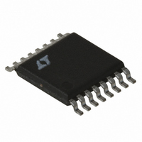
LT1976IFE Linear Technology, LT1976IFE Datasheet - Page 22

LT1976IFE
Manufacturer Part Number
LT1976IFE
Description
IC REG SW STEP-DWN 1.5A 16-TSSOP
Manufacturer
Linear Technology
Type
Step-Down (Buck)r
Datasheet
1.LT1976IFEPBF.pdf
(28 pages)
Specifications of LT1976IFE
Internal Switch(s)
Yes
Synchronous Rectifier
No
Number Of Outputs
1
Voltage - Output
1.2 ~ 54 V
Current - Output
1.5A
Frequency - Switching
200kHz
Voltage - Input
3.3 ~ 60 V
Operating Temperature
-40°C ~ 125°C
Mounting Type
Surface Mount
Package / Case
16-TSSOP Exposed Pad, 16-eTSSOP, 16-HTSSOP
Lead Free Status / RoHS Status
Contains lead / RoHS non-compliant
Power - Output
-
Available stocks
Company
Part Number
Manufacturer
Quantity
Price
Part Number:
LT1976IFE
Manufacturer:
LINEAR/凌特
Quantity:
20 000
Part Number:
LT1976IFE#PBF
Manufacturer:
LT凌特厂
Quantity:
20 000
LT1976/LT1976B
APPLICATIO S I FOR ATIO
(I
voltage on the external capacitor reaches an internal clamp
(V
22
CT
CT
100k TO V
500mV/DIV
500mV/DIV
) from the C
), the PG pin becomes a high impedance node. The
2V/DIV
V
V
SHDN
V
OUT
PG
CT
IN
PG at 80% V
T
V
pin into the external capacitor. When the
OUT
Figure 9. Power Good
LT1976
LT1976
U
PGFB
PGFB
Disconnect at 80% V
V
with 100ms Delay
V
TIME (10ms/DIV)
PG
PG
FB
C
FB
C
IN
IN
T
T
U
OUT
with 100ms Delay
0.27μF
0.27μF
200k
W
200k
153k
12k
100k
153k
12k
100k
OUT
1976 F09
C
C
Figure 10. Power Good Circuits
OUT
OUT
V
U
OUT
= 3.3V
V
OUT
= 3.3V
V
resultant PG delay time is given by t = C
the voltage on the PGFB pin drops below its V
be discharged rapidly and PG will be active low with a
200μA sink capability. If the SHDN pin is taken below its
threshold during normal operation, the C
discharged and PG inactive, resulting in a non Power Good
cycle when SHDN is taken above its threshold. Figure 9
shows the power good operation with PGFB connected to
FB and the capacitance on C
a limited amount of drive capability and is susceptible to
noise during start-up and Burst Mode operation. If erratic
operation occurs during these conditions a small filter
capacitor from the PGOOD pin to ground will ensure
proper operation. Figure 10 shows several different con-
figurations for the LT1976 Power Good circuitry.
OUT
PG at V
LT1976
LT1976
Disconnect 3.3V Logic Signal
PGFB
PGFB
IN
with 100μs Delay
V
V
PG
PG
FB
C
FB
C
IN
IN
> 4V with 100ms Delay
T
T
511k
200k
0.27μF
270pF
200k
200k
165k
100k
866k
100k
1976 F10
T
C
OUT
= 0.1μF. The PGOOD pin has
C
V
OUT
OUT
= 3.3V
V
OUT
= 12V
CT
• (V
T
PGFB
pin will be
CT
)/(I
, C
CT
CT
1976bfg
). If
will


