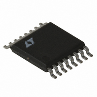
LT1976IFE Linear Technology, LT1976IFE Datasheet - Page 25

LT1976IFE
Manufacturer Part Number
LT1976IFE
Description
IC REG SW STEP-DWN 1.5A 16-TSSOP
Manufacturer
Linear Technology
Type
Step-Down (Buck)r
Datasheet
1.LT1976IFEPBF.pdf
(28 pages)
Specifications of LT1976IFE
Internal Switch(s)
Yes
Synchronous Rectifier
No
Number Of Outputs
1
Voltage - Output
1.2 ~ 54 V
Current - Output
1.5A
Frequency - Switching
200kHz
Voltage - Input
3.3 ~ 60 V
Operating Temperature
-40°C ~ 125°C
Mounting Type
Surface Mount
Package / Case
16-TSSOP Exposed Pad, 16-eTSSOP, 16-HTSSOP
Lead Free Status / RoHS Status
Contains lead / RoHS non-compliant
Power - Output
-
Available stocks
Company
Part Number
Manufacturer
Quantity
Price
Part Number:
LT1976IFE
Manufacturer:
LINEAR/凌特
Quantity:
20 000
Part Number:
LT1976IFE#PBF
Manufacturer:
LT凌特厂
Quantity:
20 000
APPLICATIO S I FOR ATIO
HIGH TEMPERATURE OPERATION
Extreme care must be taken when designing LT1976
applications to operate at high ambient temperatures. The
LT1976H grade is designed to work at elevated tempera-
tures but erratic operation can occur due to external
components. Each passive component should be checked
for absolute value and voltage ratings to ensure loop
stability at temperature. Boost and Catch diode leakages,
as well as increased series resistance (Table 5), will
adversely affect efficiency and low quiescent current op-
eration. Junction temperature increase in the diodes due
to self heating (leakage) and power dissipation should be
measured to ensure their maximum temperature specifi-
cations are not violated.
Input Voltage vs Operating Frequency Considerations
The absolute maximum input supply voltage for the LT1976
is specified at 60V. This is based solely on internal semi-
conductor junction breakdown effects. Due to internal
power dissipation the actual maximum V
particular application may be less than this.
A detailed theoretical basis for estimating internal power
loss is given in the section Thermal Considerations. Note
that AC switching loss is proportional to both operating
frequency and output current. The majority of AC switch-
ing loss is also proportional to the square of input voltage.
For example, while the combination of V
5V at 1A and f
simultaneously raising V
not possible. Nevertheless, input voltage transients up to
60V can usually be accommodated, assuming the result-
ing increase in internal dissipation is of insufficient time
duration to raise die temperature significantly.
A second consideration is controllability. A potential limi-
tation occurs with a high step-down ratio of V
as this requires a correspondingly narrow minimum switch
on time. An approximate expression for this (assuming
continuous mode operation) is given as follows:
t
ON(MIN)
= V
OUT
OSC
+ V
U
= 200kHz may be easily achievable,
F
/V
IN
IN
U
(f
to 60V and f
OSC
)
W
OSC
IN
IN
achievable in a
= 40V, V
to 700kHz is
IN
U
to V
OUT
OUT
=
,
where:
A potential controllability problem arises if the LT1976 is
called upon to produce an on time shorter than it is able to
produce. Feedback loop action will lower then reduce the
V
skipping or Burst Mode behavior is exhibited.
In summary:
1. Be aware that the simultaneous requirements of high
2. The simultaneous requirements of high V
FREQUENCY COMPENSATION
Before starting on the theoretical analysis of frequency
response the following should be remembered—the worse
the board layout, the more difficult the circuit will be to
stabilize. This is true of almost all high frequency analog
circuits. Read the Layout Considerations section first.
Common layout errors that appear as stability problems
are distant placement of input decoupling capacitor and/or
catch diode and connecting the V
ground track carrying significant switch current. In addi-
tion the theoretical analysis considers only first order non-
ideal component behavior. For these reasons, it is important
that a final stability check is made with production layout
and components.
C
V
V
V
f
V
practice due to internal dissipation. The Thermal Con-
siderations section offers a basis to estimate internal
power. In questionable cases a prototype supply should
be built and exercised to verify acceptable operation.
and high f
minimum switch on time. Cycle-skipping and/or Burst
Mode behavior will result although correct output volt-
age is usually maintained.
control voltage to the point where some sort of cycle-
OSC
IN
OUT
F
IN
= Schottky diode forward drop
, high I
= input voltage
= switching frequency
= output voltage
OUT
OSC
and high f
can result in an unacceptably short
LT1976/LT1976B
OSC
may not be achievable in
C
compensation to a
IN
, low V
25
1976bfg
OUT


