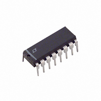
LTC1149CN-5#PBF Linear Technology, LTC1149CN-5#PBF Datasheet - Page 11

LTC1149CN-5#PBF
Manufacturer Part Number
LTC1149CN-5#PBF
Description
IC SW REG STEP-DOWN 5V 16-DIP
Manufacturer
Linear Technology
Type
Step-Down (Buck)r
Datasheet
1.LTC1149CNPBF.pdf
(20 pages)
Specifications of LTC1149CN-5#PBF
Internal Switch(s)
No
Synchronous Rectifier
Yes
Number Of Outputs
1
Voltage - Output
5V
Current - Output
50mA
Frequency - Switching
250kHz
Voltage - Input
0 ~ 48 V
Operating Temperature
0°C ~ 70°C
Mounting Type
Through Hole
Package / Case
16-DIP (0.300", 7.62mm)
Lead Free Status / RoHS Status
Lead free / RoHS Compliant
Power - Output
-
Available stocks
Company
Part Number
Manufacturer
Quantity
Price
APPLICATIO S I FOR ATIO
output ripple at low frequencies will be large enough to trip
the voltage comparator. This causes the Burst Mode
operation to be activated when the LTC1149 series would
normally be in continuous operation. The effect is most
pronounced with low values of R
improved by operating at higher frequencies with lower
values of L. The output remains in regulation at all times.
Checking Transient Response
Switching regulators take several cycles to respond to a
step in DC (resistive) load current. When a load step
occurs, V
where ESR is the effective series resistance of C
I
LOAD
>2V = SHUTDOWN
+
also begins to charge or discharge C
1k
OUT
0V = NORMAL
3300pF
1 F
1000
800
400
200
600
Figure 4. Minimum Suggested C
shifts by an amount equal to ( I
0
0
1N4148
R
0.068 F
SENSE
U U
C
200pF
T
1
L = 50 H
(V
= 0.05
IN
– V
SHDN2
I
C
CAP
V
V
TH
T
CC
CC
L = 50 H
R
L = 25 H
R
2
OUT
SENSE
SENSE
) VOLTAGE (V)
LTC1149
Figure 5. High Efficiency Step-Down Regulator with V
GNDS
= 0.02
= 0.02
V
3
IN
SENSE
SENSE
W
PDRIVE
NGATE
PGATE
SENSE
V
4
FB
+
–
OUT
1149 F04
and can be
OUT
LOAD
5
1N4148
0.047 F
100pF
1000pF
U
until the
)(ESR),
V
VALUES SHOWN FOR V
OUT
OUT
= 1.25 1 + R2
V
.
IN
IRF9Z34
IRFZ34
regulator loop adapts to the current change and returns
V
V
would indicate a stability problem. The Pin 7 external
components shown in the Figure 1 circuit will prove
adequate compensation for most applications.
A second, more severe transient is caused by switching in
loads with large (>1 F) supply bypass capacitors. The
discharged bypass capacitors are effectively put in parallel
with C
deliver enough current to prevent this problem if the load
switch resistance is low and it is driven quickly. The only
solution is to limit the rise time of the switch drive so that
the load rise time is limited to approximately (25)(C
Thus a 10 F capacitor would require a 250 s rise time,
limiting the charging current to about 200mA.
LTC1149 Adjustable Applications
When an output voltage other than 3.3V or 5V is required,
the LTC1149 adjustable version is used with an external
resistive divider from V
voltage is determined:
In applications where V
internally regulated V
R1
OUT
OUT
V
OUT
OUT
to its steady state value. During this recovery time
+
can be monitored for overshoot or ringing which
OUT
= 12V
= 1.25 1 + R2
1N5819
, causing a rapid drop in V
150 F
50V
100 H
LTC1149-3.3/LTC1149-5
OUT
R2
215k
1%
R1
25k
1%
CC
> V
R1
voltage, R
OUT
CC
OUT
+
to V
is greater than the LTC1149
R
0.05
SENSE
150 F
16V
OS-CON
FB
SENSE
Pin 10. The regulated
OUT
V
. No regulator can
must be moved to
OUT
LTC1149
CONNECTION
GROUND
OUTPUT
LOAD
1149 F05
11
LOAD
).


