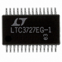
LTC3727EG-1#PBF Linear Technology, LTC3727EG-1#PBF Datasheet - Page 23

LTC3727EG-1#PBF
Manufacturer Part Number
LTC3727EG-1#PBF
Description
IC REG STEP DOWN SYNC 28SSOP
Manufacturer
Linear Technology
Series
PolyPhase®r
Type
Step-Down (Buck)r
Datasheet
1.LTC3727EGPBF.pdf
(32 pages)
Specifications of LTC3727EG-1#PBF
Internal Switch(s)
No
Synchronous Rectifier
Yes
Number Of Outputs
2
Voltage - Output
0.8 ~ 14 V
Current - Output
25A
Frequency - Switching
250kHz ~ 550kHz
Voltage - Input
4 ~ 36 V
Operating Temperature
-40°C ~ 85°C
Mounting Type
Surface Mount
Package / Case
28-SSOP
Lead Free Status / RoHS Status
Lead free / RoHS Compliant
Power - Output
-
Available stocks
Company
Part Number
Manufacturer
Quantity
Price
APPLICATIO S I FOR ATIO
which excludes MOSFET driver and control currents; the
second is the current drawn from the 3.3V linear regulator
output. V
2. INTV
control currents. The MOSFET driver current results from
switching the gate capacitance of the power MOSFETs.
Each time a MOSFET gate is switched from low to high to
low again, a packet of charge dQ moves from INTV
ground. The resulting dQ/dt is a current out of INTV
is typically much larger than the control circuit current. In
continuous mode, I
are the gate charges of the topside and bottom side
MOSFETs.
Supplying INTV
from an output-derived source will scale the V
required for the driver and control circuits by a factor of
(Duty Cycle)/(Efficiency). For example, in a 20V to 5V
application, 10mA of INTV
mately 2.5mA of V
loss from 10% or more (if the driver was powered directly
from V
3. I
fuse (if used), MOSFET, inductor, current sense resistor,
and input and output capacitor ESR. In continuous mode
the average output current flows through L and R
but is “chopped” between the topside MOSFET and the
synchronous MOSFET. If the two MOSFETs have approxi-
mately the same R
MOSFET can simply be summed with the resistances of L,
R
R
= 40mΩ (sum of both input and output capacitance
losses), then the total resistance is 130mΩ. This results in
losses ranging from 3% to 13% as the output current
increases from 1A to 5A for a 5V output, or a 4% to 20%
loss for a 3.3V output. Efficiency varies as the inverse
square of V
output power level. The combined effects of increasingly
lower output voltages and higher currents required by
high performance digital systems is not doubling but
quadrupling the importance of loss terms in the switching
regulator system!
SENSE
DS(ON)
2
R losses are predicted from the DC resistances of the
IN
and ESR to obtain I
CC
= 30mΩ, R
) to only a few percent.
IN
current is the sum of the MOSFET driver and
current typically results in a small (<0.1%) loss.
OUT
CC
for the same external components and
IN
power through the EXTV
GATECHG
U
L
current. This reduces the mid-current
DS(ON)
= 50mΩ, R
U
2
, then the resistance of one
CC
R losses. For example, if each
=f(Q
current results in approxi-
T
SENSE
+ Q
W
B
), where Q
= 10mΩ and R
CC
switch input
U
IN
T
current
and Q
CC
SENSE
CC
that
ESR
to
B
,
4. Transition losses apply only to the topside MOSFET(s),
and become significant only when operating at high input
voltages (typically 15V or greater). Transition losses can
be estimated from:
Other “hidden” losses such as copper trace and internal
battery resistances can account for an additional 5% to
10% efficiency degradation in portable systems. It is very
important to include these “system” level losses during
the design phase. The internal battery and fuse resistance
losses can be minimized by making sure that C
adequate charge storage and very low ESR at the switch-
ing frequency. A 25W supply will typically require a mini-
mum of 22μF to 47μF of capacitance having a maximum
of 20mΩ to 50mΩ of ESR. The LTC3727 2-phase architec-
ture typically halves this input capacitance requirement
over competing solutions. Other losses, including Schot-
tky diode conduction losses during dead-time and induc-
tor core losses, generally account for less than 2% total
additional loss.
Checking Transient Response
The regulator loop response can be checked by looking at
the load current transient response. Switching regulators
take several cycles to respond to a step in DC (resistive)
load current. When a load step occurs, V
amount equal to ΔI
series resistance of C
discharge C
forces the regulator to adapt to the current change and
return V
time V
ringing, which would indicate a stability problem. OPTI-
LOOP compensation allows the transient response to be
optimized over a wide range of output capacitance and
ESR values. The availability of the I
optimization of control loop behavior but also provides a
DC coupled and AC filtered closed loop response test
point. The DC step, rise time and settling at this test point
truly reflects the closed loop response . Assuming a pre-
dominantly second order system, phase margin and/or
damping factor can be estimated using the percentage of
Transition Loss = (1.7) V
OUT
OUT
can be monitored for excessive overshoot or
OUT
to its steady-state value. During this recovery
generating the feedback error signal that
LTC3727/LTC3727-1
LOAD
OUT
(ESR), where ESR is the effective
. ΔI
IN
LOAD
2
I
O(MAX)
also begins to charge or
TH
pin not only allows
C
RSS
OUT
f
shifts by an
23
IN
3727fc
has


