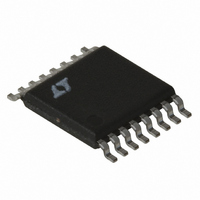
LT3431EFE Linear Technology, LT3431EFE Datasheet - Page 23

LT3431EFE
Manufacturer Part Number
LT3431EFE
Description
IC SW REG STEP-DOWN 3A 16TSSOP
Manufacturer
Linear Technology
Type
Step-Down (Buck)r
Datasheet
1.LT3431EFEPBF.pdf
(28 pages)
Specifications of LT3431EFE
Internal Switch(s)
Yes
Synchronous Rectifier
No
Number Of Outputs
1
Voltage - Output
1.2 ~ 48 V
Current - Output
3A
Frequency - Switching
500kHz
Voltage - Input
5.5 ~ 60 V
Operating Temperature
-40°C ~ 125°C
Mounting Type
Surface Mount
Package / Case
16-TSSOP Exposed Pad, 16-eTSSOP, 16-HTSSOP
Lead Free Status / RoHS Status
Contains lead / RoHS non-compliant
Power - Output
-
Available stocks
Company
Part Number
Manufacturer
Quantity
Price
Part Number:
LT3431EFE
Manufacturer:
LINEAR/凌特
Quantity:
20 000
Part Number:
LT3431EFE#PBF
Manufacturer:
LT/凌特
Quantity:
20 000
Part Number:
LT3431EFE#TRPBF
Manufacturer:
LINEAR/凌特
Quantity:
20 000
APPLICATIO S I FOR ATIO
BUCK CONVERTER WITH ADJUSTABLE SOFT-START
Large capacitive loads or high input voltages can cause
high input currents at start-up. Figure 13 shows a circuit
that limits the dv/dt of the output at start-up, controlling
the capacitor charge rate. The buck converter is a typical
configuration with the addition of R3, R4, C
As the output starts to rise, Q1 turns on, regulating switch
current via the V
output. Output rise time is controlled by the current
through C
is in regulation, Q1 turns off and the circuit operates
normally. R3 is transient protection for the base of Q1.
Using the values shown in Figure 10,
The ramp is linear and rise times in the order of 100ms are
possible. Since the circuit is voltage controlled, the ramp
rate is unaffected by load characteristics and maximum
output current is unchanged. Variants of this circuit can be
used for sequencing multiple regulator outputs.
INPUT
12V
Rise Time
Rise Time
Figure 13. Buck Converter with Adjustable Soft-Start
C3
4.7 F
25V
CER
SS
defined by R4 and Q1’s V
V
SHDN
SYNC
IN
0.022 F
BOOST
C
R
LT3431
47 10
C
3.3k
GND
C
R
pin to maintain a constant dv/dt at the
4
C
U
•
BIAS
C
V
SW
FB
C
SS
V
3
BE
C
220pF
F
U
0.22 F
0 7
15 10
C2
V
.
D1
30BQ060
OR B250A
Q1
OUT
•
MMSD914TI
15 H
D2
–
L1
R4
47k
W
100 F
9
R3
2k
10V
L1: CDRH104R-220M
C1
BE
15nF
5
+
C
SS
. Once the output
5
R1
15.4k
R2
4.99k
ms
3431 F13
SS
U
and Q1.
OUTPUT
5V
2A
Dual Polarity Output Converter
The circuit in Figure 14a generates both positive and
negative 5V outputs with all components under 3mm
height. The topology for the 5V output is a standard buck
converter. The –5V output uses a second inductor L2,
diode D3, and output capacitor C6. The capacitor C4
couples energy to L2 and ensures equal voltages across
L2 and L1 during steady state. Instead of using a trans-
former for L1 and L2, uncoupled inductors were used
because they require less height than a single transformer,
can be placed separately in the circuit layout for optimized
space savings and reduce overall cost. This is true even
when the uncoupled inductors are sized (twice the value of
inductance of the transformer) in order to keep ripple
current comparable to the transformer solution. If a single
transformer becomes available to provide a better height
/cost solution, refer to the Dual Output SEPIC circuit
description in Design Note 100 for correct transformer
connection.
During switch on-time, in steady state, the voltage across
both L1 and L2 is positive and equal ; with energy (and
current) ramping up in each inductor. The current in L2 is
provided by the coupling capacitor C4. During switch off-
time, current ramps downward in each inductor. The
current in L2 and C4 flows via the catch diode D3, charging
the negative output capacitor C6. If the negative output is
not loaded enough it can go severely unregulated (become
more negative). Figure 14b shows the maximum allow-
able –5V output load current (vs load current on the 5V
output) that will maintain the –5V output within 3%
tolerance. Figure 14c shows the –5V output voltage regu-
lation versus its own load current when plotted for three
separate load currents on the 5V output. The efficiency of
the dual polarity output converter circuit shown in Figure
14a is given in Figure 14d.
LT3431
sn3431 3431fs
23


