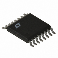
LT3431EFE#TRPBF Linear Technology, LT3431EFE#TRPBF Datasheet - Page 15

LT3431EFE#TRPBF
Manufacturer Part Number
LT3431EFE#TRPBF
Description
IC SW REG STEP-DOWN 3A 16TSSOP
Manufacturer
Linear Technology
Type
Step-Down (Buck)r
Datasheet
1.LT3431EFEPBF.pdf
(28 pages)
Specifications of LT3431EFE#TRPBF
Internal Switch(s)
Yes
Synchronous Rectifier
No
Number Of Outputs
1
Voltage - Output
1.2 ~ 48 V
Current - Output
3A
Frequency - Switching
500kHz
Voltage - Input
5.5 ~ 60 V
Operating Temperature
-40°C ~ 125°C
Mounting Type
Surface Mount
Package / Case
16-TSSOP Exposed Pad, 16-eTSSOP, 16-HTSSOP
Lead Free Status / RoHS Status
Lead free / RoHS Compliant
Power - Output
-
Available stocks
Company
Part Number
Manufacturer
Quantity
Price
APPLICATIO S I FOR ATIO
If tantalum capacitors are used, values in the 22 F to
470 F range are generally needed to minimize ESR and
meet ripple current and surge ratings. Care should be
taken to ensure the ripple and surge ratings are not
exceeded. The AVX TPS and Kemet T495 series are surge
rated. AVX recommends derating capacitor operating
voltage by 2:1 for high surge applications.
CATCH DIODE
Highest efficiency operation requires the use of a Schottky
type diode. DC switching losses are minimized due to its
low forward voltage drop, and AC behavior is benign due
to its lack of a significant reverse recovery time. Schottky
diodes are generally available with reverse voltage ratings
of up to 60V and even 100V, and are price competitive with
other types.
The use of so-called “ultrafast” recovery diodes is gener-
ally not recommended. When operating in continuous
mode, the reverse recovery time exhibited by “ultrafast”
diodes will result in a slingshot type effect. The power
internal switch will ramp up V
attempt to get it to recover. Then, when the diode has
finally turned off, some tens of nanoseconds later, the V
node voltage ramps up at an extremely high dV/dt, per-
haps 5 to even 10V/ns ! With real world lead inductances,
the V
result in poor RFI behavior and if the overshoot is severe
enough, damage the IC itself.
The suggested catch diode (D1) is an International Recti-
fier 30BQ060 Schottky. It is rated at 3A average forward
current and 60V reverse voltage. Typical forward voltage
is 0.52V at 3A. The diode conducts current only during
switch off time. Peak reverse voltage is equal to regulator
input voltage. Average forward current in normal opera-
tion can be calculated from:
This formula will not yield values higher than 3A with
maximum load current of 3A.
I
D AVG
(
SW
node can easily overshoot the V
)
I
OUT
V
U
IN
V
IN
–
V
OUT
U
IN
current into the diode in an
W
IN
rail. This can
U
SW
BOOST PIN
For most applications, the boost components are a 0.22 F
capacitor and a MMSD914TI diode. The anode is typically
connected to the regulated output voltage to generate a
voltage approximately V
stage. However, the output stage discharges the boost
capacitor during the on time of the switch. The output
driver requires at least 3V of headroom throughout this
period to keep the switch fully saturated. If the output
voltage is less than 3.3V, it is recommended that an
alternate boost supply is used. The boost diode can be
connected to the input, although, care must be taken to
prevent the 2 V
BOOST pin absolute maximum rating. The additional
voltage across the switch driver also increases power
loss, reducing efficiency. If available, an independent
supply can be used with a local bypass capacitor.
A 0.22 F boost capacitor is recommended for most appli-
cations. Almost any type of film or ceramic capacitor is
suitable, but the ESR should be <1 to ensure it can be
fully recharged during the off time of the switch. The
capacitor value is derived from worst-case conditions of
1840ns on time, 75mA boost current and 0.7V discharge
ripple. The boost capacitor value could be reduced under
less demanding conditions, but this will not improve
circuit operation or efficiency. Under low input voltage and
low load conditions, a higher value capacitor will reduce
discharge ripple and improve start-up operation.
SHUTDOWN FUNCTION AND UNDERVOLTAGE
LOCKOUT
Figure 4 shows how to add undervoltage lockout (UVLO)
to the LT3431. Typically, UVLO is used in situations where
the input supply is current limited , or has a relatively high
source resistance. A switching regulator draws constant
power from the source, so source current increases as
source voltage drops. This looks like a negative resistance
load to the source and can cause the source to current limit
or latch low under low source voltage conditions. UVLO
prevents the regulator from operating at source voltages
where these problems might occur.
IN
boost voltage from exceeding the
OUT
above V
IN
to drive the output
LT3431
sn3431 3431fs
15


