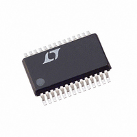
LTC1142HVCG Linear Technology, LTC1142HVCG Datasheet - Page 4

LTC1142HVCG
Manufacturer Part Number
LTC1142HVCG
Description
IC SW REG STEP-DOWN DUAL 28-SSOP
Manufacturer
Linear Technology
Type
Step-Down (Buck)r
Datasheet
1.LTC1142CG.pdf
(20 pages)
Specifications of LTC1142HVCG
Internal Switch(s)
No
Synchronous Rectifier
Yes
Number Of Outputs
2
Voltage - Output
3.3V, 5V
Current - Output
50mA
Frequency - Switching
250kHz
Voltage - Input
3.5 ~ 18 V
Operating Temperature
0°C ~ 70°C
Mounting Type
Surface Mount
Package / Case
28-SSOP
Lead Free Status / RoHS Status
Contains lead / RoHS non-compliant
Power - Output
-
Available stocks
Company
Part Number
Manufacturer
Quantity
Price
Part Number:
LTC1142HVCG
Manufacturer:
LINEAR/凌特
Quantity:
20 000
Part Number:
LTC1142HVCG-ADJ
Manufacturer:
LT/凌特
Quantity:
20 000
LTC1142/LTC1142L/LTC1142HV
ELECTRICAL CHARACTERISTICS
SYMBOL
V
t
Note 1: Absolute Maximum Ratings are those values beyond which the life
of a device may be impaired.
Note 2: T
dissipation P
Note 3: This current is for one regulator block. Total supply current is the
sum of Pins 10 and 24 currents. Dynamic supply current is higher due to
the gate charge being delivered at the switching frequency. See the
Applications Information section.
TYPICAL PERFOR A CE CHARACTERISTICS
4
OFF
SHDN
100
100
95
90
85
98
96
94
92
90
88
86
84
82
80
0.01
0
5V Output Efficiency
3.3V Efficiency vs Input Voltage
J
LTC1142CG: T
is calculated from the ambient temperature T
D
PARAMETER
Shutdown Pin Threshold
Off-Time (Note 4)
I
according to the following formula:
LOAD
4
LOAD CURRENT (A)
= 100mA
INPUT VOLTAGE (V)
V
V
IN
IN
8
0.1
= 10V
= 6V
J
= T
FIGURE 1 CIRCUIT
V
A
OUT
I
12
LOAD
+ (P
= 3.3V
= 1A
D
W
16
95 C/ W)
1
1142 G01
1142 G04
U
20
2
CONDITIONS
LTC1142, LTC1142HV
C
T
A
100
– 10
– 20
– 30
– 40
= 390pF, I
V
V
and power
95
90
85
40
30
20
10
14
14
0
0.01
3.3V Output Efficiency
Line Regulation
0
= V
= V
FIGURE 1 CIRCUIT
I
LOAD
OUT
OUT
LOAD
= 1A
4
+ 100mV (Forced)
– 100mV (Forced)
– 40 C T
= 700mA
LOAD CURRENT (A)
INPUT VOLTAGE (V)
V
V
IN
IN
8
0.1
= 10V
= 5V
A
Note 4: In applications where R
time increases approximately 40%.
Note 5: The LTC1142/LTC1142L/LTC1142HV are guaranteed to meet
specified performance from 0 C to 70 C and are designed, characterized
and expected to meet these extended temperature limits, but are not tested
at – 40 C and 85 C. Guaranteed I-grade parts are available, consult the
factory.
Note 6: The LTC1142L-ADJ allows operation down to V
12
85 C (Note 5), V
16
1
1142 G02
1142 G05
20
2
10
= V
– 100
–20
– 40
– 60
– 80
100
24
98
96
94
92
90
88
86
84
82
80
20
SENSE
0
= 10V, unless otherwise noted.
5V Efficiency vs Input Voltage
0
0
Load Regulation
is placed at ground potential, the off-
0.5
MIN
0.55
125
3.8
4
V
V
OUT
OUT
I
V
LOAD
INPUT VOLTAGE (V)
IN
LOAD CURRENT (A)
V
= 5V
= 3.3V
= 6V
IN
1.0
= 100mA
8
TYP
150
0.8
= 6V
25
5
FIGURE 1 CIRCUIT
R
FIGURE 1 CIRCUIT
V
IN
SENSE
1.5
OUT
12
= 3.5V.
MAX
175
I
2
6
= 5V
LOAD
V
= 0.05
IN
V
= 12V
IN
2.0
16
= 1A
= 12V
UNITS
1142 G03
1142 G06
mV
mV
2.5
20
V
s


