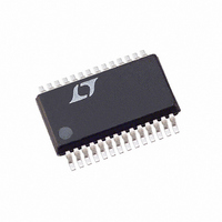
LTC1142HVCG-ADJ Linear Technology, LTC1142HVCG-ADJ Datasheet

LTC1142HVCG-ADJ
Specifications of LTC1142HVCG-ADJ
Available stocks
Related parts for LTC1142HVCG-ADJ
LTC1142HVCG-ADJ Summary of contents
Page 1
... The LTC1142 series is ideal for applications requiring dual output voltages with high conversion efficiencies over a wide load current range in a small amount of board space. , LTC and LT are registered trademarks of Linear Technology Corporation. Burst Mode is a trademark of Linear Technology Corporation 5.2V TO 18V 0V = NORMAL > ...
Page 2
... V < 12V, 6V < V < 12V 2.1V, 4V < < 12V SD1 SD2 10 24 TOP VIEW ORDER PART – 28 SENSE 1 NUMBER 27 I TH1 26 INTV CC1 LTC1142HVCG-ADJ 24 V IN1 LTC1142LCG-ADJ 23 PDRIVE NDRIVE PGND2 18 SGND2 17 SHDN2 16 V FB2 + SENSE PACKAGE = 95 C unless otherwise noted. MIN ...
Page 3
ELECTRICAL CHARACTERISTICS temperature range, otherwise specifications are at T SYMBOL PARAMETER Input DC Supply Current (Note 3) Normal Mode Sleep Mode Shutdown Input DC Supply Current (Note 3) Normal Mode Sleep Mode Shutdown V – V Current Sense Threshold Voltage ...
Page 4
LTC1142/LTC1142L/LTC1142HV ELECTRICAL CHARACTERISTICS SYMBOL PARAMETER V Shutdown Pin Threshold SHDN t Off-Time (Note 4) OFF Note 1: Absolute Maximum Ratings are those values beyond which the life of a device may be impaired. Note calculated from the ...
Page 5
W U TYPICAL PERFOR A CE CHARACTERISTICS DC Supply Current 2.1 1.8 ACTIVE MODE 1.5 1.2 PER REGULATOR BLOCK NOT INCLUDING 0.9 GATE CHARGE CURRENT PINS 10, 24 0.6 0.3 SLEEP MODE ...
Page 6
LTC1142/LTC1142L/LTC1142HV CTIO S NC (Pins 7, 8): No Connection. PDRIVE 5 (Pin 9): High Current Drive for Top P-Channel MOSFET, 5V Section. Voltage swing at this pin is from V to ground. V (Pin 10): ...
Page 7
CTIO S NDRIVE 1 (Pin 6): High Current Drive for Bottom N-Channel MOSFET, Section 1. Voltage swing at Pin 6 is from ground IN1 NC (Pins 7, 8): No Connection. PDRIVE 2 ...
Page 8
LTC1142/LTC1142L/LTC1142HV CTIO AL DIAGRA Only one regulator block shown. Pin numbers are for 3.3V (5V) sections for LTC1142/LTC1142HV, and for LTC1142L-ADJ/LTC1142HV-ADJ. OUT1 OUT2 PIN NUMBERS FOR 2(16) LTC1142, LTC1142HV LTC1142-ADJ PIN NUMBERS 3(17) FOR ...
Page 9
U OPERATIO Refer to Functional Diagram As the load current increases, the output voltage de- creases slightly. This causes the output of the gain stage [Pin 27(13)] to increase the current comparator thresh- old, thus tracking the load current. The ...
Page 10
LTC1142/LTC1142L/LTC1142HV U U APPLICATIO S I FOR ATIO both track I . Once R has been chosen, I MAX SENSE I can be predicted from the following: SC(PK) 15mV I BURST R SENSE 150mV I = SC(PK) R SENSE The ...
Page 11
U U APPLICATIO S I FOR ATIO eased at the expense of efficiency. If too small an inductor is used, the inductor current will decrease past zero and change polarity. A consequence of this is that the LTC1142 may not ...
Page 12
LTC1142/LTC1142L/LTC1142HV U U APPLICATIO S I FOR ATIO dead-time, which could cost as much efficiency (although there are no other harmful effects if D1 and D2 are omitted). Therefore, D1 and D2 should be selected for a ...
Page 13
U U APPLICATIO S I FOR ATIO current. When a load step occurs, V amount equal to I • ESR, where ESR is the effective LOAD series resistance OUT LOAD or discharge C until the regulator ...
Page 14
LTC1142/LTC1142L/LTC1142HV U U APPLICATIO S I FOR ATIO Figure 5 shows how the efficiency losses in one section of a typical LTC1142 regulator end up being apportioned. The gate charge loss is responsible for the majority of the efficiency lost ...
Page 15
U U APPLICATIO S I FOR ATIO To prevent stray pickup a 100pF capacitor is suggested across R1 located close to the LTC1142HV-ADJ/LTC1142L- ADJ as in Figure 6. The external divider network must be placed across C with the negative ...
Page 16
LTC1142/LTC1142L/LTC1142HV U U APPLICATIO S I FOR ATIO ing with Kelvin connections. Be sure to use a PCB pattern similar to that shown in Figure 7 for the current sense resistors. 4. Does the (+) plate of C connect to ...
Page 17
U U APPLICATIO S I FOR ATIO may be loaded without regard to the primary output load, providing that the loop remains in continuous mode operation. Burst Mode operation can be suppressed at low output currents with a simple external ...
Page 18
LTC1142/LTC1142L/LTC1142HV U TYPICAL APPLICATIO IN1 22 F 0.22 F 35V 2 P-CH Si9430DY L1 R SENSE1 33 H 0.075 V OUT1 2.5V/1.5A 1000pF + C OUT1 220 F 10V D1 N- MBRS130T3 Si9410DY 49.9k 1% ...
Page 19
... Figure 15. LTC1142HV-ADJ High Efficiency Power Supply Providing 3.3V/2A with Built-In Battery Charger Information furnished by Linear Technology Corporation is believed to be accurate and reliable. However, no responsibility is assumed for its use. Linear Technology Corporation makes no represen- tation that the interconnection of its circuits as described herein will not infringe on existing patent rights. ...
Page 20
... Desktop VID Programmable Synch Switching Reg LTC1873 Dual Synchronous Switching Regulator with 5-Bit Desktop VID LTC1929 2-Phase, Synchronous High Efficiency Converter trademark of Linear Technology Corporation. Pentium is a registered trademark of Intel Corporation. SENSE Linear Technology Corporation 20 1630 McCarthy Blvd., Milpitas, CA 95035-7417 (408) 432-1900 FAX: (408) 434-0507 www.linear-tech.com ...


