LM26420YSQ/NOPB National Semiconductor, LM26420YSQ/NOPB Datasheet
LM26420YSQ/NOPB
Specifications of LM26420YSQ/NOPB


Related parts for LM26420YSQ/NOPB

LM26420YSQ/NOPB Summary of contents
Page 1
... Additional features include internal soft-start circuitry to re- duce inrush current, pulse-by-pulse current limit, thermal shutdown, power good indicators, precision enables, and out- put over-voltage protection. Typical Application Circuit © 2010 National Semiconductor Corporation LM26420 Features ■ Input voltage range of 3.0V to 5.5V ■ ...
Page 2
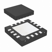
Connection Diagrams 16-Pin LLP (TOP VIEW) Ordering Information Frequency Order Number Option LM26420XMH LM26420XMHX 2.2MHz LM26420XSQ LM26420XSQX LM26420YMH LM26420YMHX 0.55MHz LM26420YSQ LM26420YSQX NOPB versions available as well www.national.com 30069601 NSC Package Package Type Drawing eTSSOP-20 MXA20A LLP-16 SQB16A eTSSOP-20 MXA20A ...
Page 3
Pin Descriptions 20-Pin eTSSOP Pin Name Function 3, 4 VIND Power Input supply for Buck 1. 1 17, 18 VIND Power Input supply for Buck VINC Input supply for control circuitry. 6,7 PGND Power ground pin for ...
Page 4
... Absolute Maximum Ratings If Military/Aerospace specified devices are required, please contact the National Semiconductor Sales Office/ Distributors for availability and specifications Voltage EN Voltage SW Voltage ESD Susceptibility Human Body Model (Note 3) Electrical Characteristics Per Buck Limits in standard type are for T = 25°C only; limits in boldface type apply over the junction temperature (T J +125° ...
Page 5
Symbol Parameter Junction to Ambient θ LFPM Air Flow (Note θ Junction to Case (Note JC T Thermal Shutdown Temperature SD Note 1: Absolute maximum ratings indicate limits beyond which damage to the device may occur. Operating Range ...
Page 6
Typical Performance Characteristics All curves taken 5.0V with configuration in typical application circuit shown in Application Information section of this IN datasheet 25°C, unless otherwise specified. J η vs Load "X" 5V, V ...
Page 7
Load "X" & 3V 1.2V IN OUT 30069688 η vs Load "X" & 3V 0.8V IN OUT 30069641 Load Regulation 1.8V (All Options) ...
Page 8
Line Regulation - "X" 1.8V, I OUT OUT Oscillator Frequency vs Temperature - "X" R TOP vs Temperature (LLP-16 Package) DSON www.national.com = 1,000mA 30069627 Oscillator Frequency vs Temperature - "Y" 30069647 R DSON 30069649 8 Line Regulation ...
Page 9
R TOP vs Temperature (eTSSOP-20 Package) DSON I (Quiescent Current Switching) - "X" Q Load Transient Response - X Version (V = 1.2V, 25-100% Load Transient) OUT R BOTTOM vs Temperature (eTSSOP-20 Package) DSON 30069691 I (Quiescent Current Switching) - ...
Page 10
Start-Up (Soft-Start 1.8V @ 1A, V OUT V vs Temperature FB Reverse Current Limit vs Temperature www.national.com = 5V) IN 30069657 30069659 30069680 10 Enable - Disable (V = 1. 5V) OUT IN 30069658 ...
Page 11
Simplified Block Diagram Per Buck FIGURE 1. 11 30069604 www.national.com ...
Page 12
Applications Information THEORY OF OPERATION The LM26420 is a constant frequency dual PWM buck syn- chronous regulator IC that delivers two 2.0A load currents. The regulator has a preset switching frequency of 2.2MHz or 550kHz. This high frequency allows the ...
Page 13
PRECISION ENABLE The LM26420 features independent precision enables that allow the converter to be controlled by an external signal. This feature allows the device to be sequenced either by a external control signal or the output of another converter in ...
Page 14
Design Guide INDUCTOR SELECTION The Duty Cycle (D) can be approximated quickly using the ratio of output voltage ( input voltage (V OUT The voltage drop across the internal NMOS (SW_BOT) and PMOS (SW_TOP) must be included to ...
Page 15
Since the duty cycles of the two channels may overlap, cal- culation of the input ripple RMS current is a little tedious. Use the following equation Channel 1's maximum output current maximum output current ...
Page 16
V = 0.80V REF FIGURE 5. Programming V To determine the maximum allowed resistor tolerance , use the following equation: where TOL is the set point accuracy of the regulator, Φ is the tolerance Example: VOUT ...
Page 17
FIGURE 9. V controlling V IN The LM26420's power good feature is design with hysterysis in order to insure no false power good flags are asserted dur- ing large transient. Once power good is asserted high, it will not be ...
Page 18
Calculating Efficiency, and Junction Temperature The complete LM26420 DC/DC converter efficiency can be calculated in the following manner. Or Calculations for determining the most significant power loss- es are shown below. Other losses totaling less than 2% are not discussed. ...
Page 19
... Once this is determined, the maximum ambient temperature allowed for a desired junction temperature can be found. An example of calculating R National Semiconductor LM26420 LLP demonstration board is shown below. The four layer PCB is constructed using FR4 with 1 oz copper traces. The copper ground plane is on the bottom layer. The ground plane is accessed by eight vias ...
Page 20
LLP Package For certain high power applications, the PCB land may be modified to a "dog bone" shape (see Figure 6). By increasing the size of ground plane, and adding thermal vias, the R www.national.com FIGURE 11. Internal LLP Connection ...
Page 21
LM26420X Design Example 1 FIGURE 13. LM26420X (2.2MHz): V Part Buck Regulator C3, C4 15µF, 6.3V, 1206, X5R C1 33µF, 6.3V, 1206, X5R C2 22µF, 6.3V, 1206, X5R C5 0.47µF, 10V, 0805, X7R L1 L2 10.0kΩ, 0603, ...
Page 22
LM26420X Design Example 2 FIGURE 14. LM26420X (2.2MHz): V Part R3 R7, R2 www.national.com = 5V 1.8V @ 2.0A and V IN OUT1 Bill ...
Page 23
LM26420X Design Example 3 FIGURE 15. LM26420X (2.2MHz): V Part Buck Regulator C3, C4 15µF, 6.3V, 1206, X5R C1 22µF, 6.3V, 1206, X5R C2 33µF, 6.3V, 1206, X5R C5 0.47µF, 10V, 0805, X7R L1, L2 10.0kΩ, 0603, ...
Page 24
LM26420Y Design Example 4 FIGURE 16. LM26420Y (550kHz): V Part ID U1 C3, C4 C1 www.national.com = 5V 1.2V @ 2.0A and V IN OUT1 ...
Page 25
LM26420Y Design Example 5 FIGURE 17. LM26420Y (550kHz): V Part Buck Regulator C3, C4 22µF, 6.3V, 1206, X5R C1, C2, C6, C7, C8 47µF, 6.3V, 1206, X5R C5 0.47µF, 10V, 0805, X7R L1 L2 10.0kΩ, 0603, 1% ...
Page 26
LM26420Y Design Example 6 FIGURE 18. LM26420Y (550kHz): V Part ID U1 C3, C4 C1, C2 L1 www.national.com = 5V 3.3V @ 2.0A and V IN OUT1 Bill ...
Page 27
Physical Dimensions inches (millimeters) unless otherwise noted 20-Lead eTSSOP Package NS Package Number MXA20A 16-Lead LLP Package NS Package Number SQB16A 27 www.national.com ...
Page 28
... For more National Semiconductor product information and proven design tools, visit the following Web sites at: www.national.com Products Amplifiers www.national.com/amplifiers Audio www.national.com/audio Clock and Timing www.national.com/timing Data Converters www.national.com/adc Interface www.national.com/interface LVDS www.national.com/lvds Power Management www.national.com/power Switching Regulators www.national.com/switchers LDOs www.national.com/ldo LED Lighting www ...