NCP1589AMNTWG ON Semiconductor, NCP1589AMNTWG Datasheet
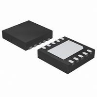
IC CTLR SYNC BUCK 1PH LV 10-DFN

NCP1589AMNTWG

Manufacturer Part Number
NCP1589AMNTWG
Description
IC CTLR SYNC BUCK 1PH LV 10-DFN
Manufacturer
ON Semiconductor
Type
Step-Down (Buck)r
Datasheet

Specifications of NCP1589AMNTWG

Internal Switch(s)
No
Synchronous Rectifier
Yes
Number Of Outputs
1
Voltage - Output
Adj to 0.8V
Current - Output
1.5A
Frequency - Switching
300kHz
Voltage - Input
4.5 ~ 13.2 V
Operating Temperature
0°C ~ 70°C
Mounting Type
Surface Mount
Package / Case
10-VFDFN Exposed Pad
Topology
Boost, Buck
Output Voltage
0.4 V
Output Current
8 mA
Switching Frequency
300 KHz
Duty Cycle (max)
80 %
Operating Supply Voltage
15 V
Supply Current
8 mA
Maximum Operating Temperature
+ 150 C
Minimum Operating Temperature
0 C
Mounting Style
SMD/SMT
Lead Free Status / RoHS Status
Lead free / RoHS Compliant
Power - Output
-

Available stocks

Company
Part Number
Manufacturer
Quantity
Price
Part Number:
NCP1589AMNTWG
Manufacturer:
ON Semiconductor
Quantity:
3 000
Part Number:
NCP1589AMNTWG
Manufacturer:
ON Semiconductor
Quantity:
500
Part Number:
NCP1589AMNTWG
Manufacturer:
ON/安森美
Quantity:
20 000
Part Number:
NCP1589AMNTWG
Manufacturer:
ON
Quantity:
7 833
Part Number:
NCP1589AMNTWG
Manufacturer:
ON
Quantity:
14 197
Company:
Part Number:
NCP1589AMNTWG
Quantity:
290
NCP1589A, NCP1589B
Product Preview
Low Voltage Synchronous
Buck Controller
from a 5 V or 12 V supply. This device is capable of producing an
output voltage as low as 0.8 V. This device is capable of converting
voltage from as low as 2.5 V. This 10−pin device provides an optimal
level of integration to reduce size and cost of the power supply.
Features include a 1.5 A gate driver design and an internally set
300 kHz or 600 kHz oscillator. In addition to the 1.5 A gate drive
capability, other efficiency enhancing features of the gate driver
include adaptive non−overlap circuitry. The NCP1589A/B also
incorporates an externally compensated error amplifier. Protection
features include programmable short circuit protection and
undervoltage lockout (UVLO).
Features
Applications
This document contains information on a product under development. ON Semiconductor
reserves the right to change or discontinue this product without notice.
© Semiconductor Components Industries, LLC, 2009
May, 2009 − Rev. P4
The NCP1589A/B is a low cost PWM controller designed to operate
V
300 kHz and 600 kHz Internal Oscillator
Boost Pin Operates to 30 V
Voltage Mode PWM Control
Precision 0.8 V Internal Reference
Adjustable Output Voltage
Internal 1.5 A Gate Drivers
80% Max Duty Cycle
Input Under Voltage Lockout
Programmable Current Limit
This is a Pb−Free Device
Graphics Cards
Desktop Computers
Servers / Networking
DSP & FPGA Power Supply
DC−DC Regulator Modules
CC
Range from 4.5 V to 13.2 V
1
NCP1589AMNTWG
NCP1589BMNTWG
NCP1589AMNTXG
NCP1589BMNTXG
†For information on tape and reel specifications,
including part orientation and tape sizes, please
refer to our Tape and Reel Packaging Specifications
Brochure, BRD8011/D.
(Note: Microdot may be in either location)
CASE 485C
BOOT
Device
GND
DFN10
UG
LG
1589x
A
L
Y
W
G
LX
ORDERING INFORMATION
PIN CONNECTIONS
http://onsemi.com
1
2
3
4
5
= Specific Device Code
x = A or B
= Assembly Location
= Wafer Lot
= Year
= Work Week
= Pb−Free Device
(Top View)
(Pb−Free)
Package
MARKING DIAGRAMS
DFN10
Publication Order Number:
10
ALYWG
1589x
9
8
7
6
G
Tape & Reel
Shipping
NCP1589A/D
PGOOD
VOS
FB
COMP/EN
V
3000 /
CC

Related parts for NCP1589AMNTWG

NCP1589AMNTWG Summary of contents

Page 1

... PIN CONNECTIONS 1 BOOT GND (Top View) ORDERING INFORMATION Device Package NCP1589AMNTWG NCP1589BMNTWG DFN10 (Pb−Free) NCP1589AMNTXG NCP1589BMNTXG †For information on tape and reel specifications, including part orientation and tape sizes, please refer to our Tape and Reel Packaging Specifications Brochure, BRD8011/D. 1 1589x ALYWG G PGOOD ...

Page 2

PGOOD COMP/ 0.0015mF 17.08kW C2 0.007mF 0.014mF R1 3.878kW R3 4.12kW 74.2W PGOOD VOS 9 MONITOR OV and UV 0 ref FB 8 − ref COMP/EN ...

Page 3

PIN FUNCTION DESCRIPTION Pin No. Symbol 1 BOOT Supply rail for the floating top gate driver. To form a boost circuit, use an external diode to bring the desired input voltage to this pin (cathode connected to BOOT pin). Connect ...

Page 4

ELECTRICAL CHARACTERISTICS 1.0 nF, for min/max values unless otherwise noted Characteristic Input Voltage Range Boost Voltage Range Supply Current Quiescent Supply Current (NCP1589A) Boost Quiescent Current Undervoltage Lockout UVLO Threshold UVLO Threshold UVLO Hysteresis ...

Page 5

T , JUNCTION TEMPERATURE (°C) J Figure 3. Oscillator Frequency (F Temperature 5.3 5.0 4.7 4.4 4.1 3.8 3 JUNCTION TEMPERATURE (°C) J Figure 5. ...

Page 6

Over Current Protection (OCP) The NCP1589A/B monitors the voltage drop across the low side mosfet and uses this information to determine if there is excessive output current. The voltage across the low side mosfet is measured from the LX pin, ...

Page 7

Internal UVLO Fault 1.45 V COMP −0.7 V 700 OCP Program- mable UG V OUT FB PGOOD POR UVLO 0 NORMAL Figure 7. Typical Startup Sequence http://onsemi.com 7 3.6 V ...

Page 8

VOS PGOOD UG LG Overvoltage Feedback and Compensation The NCP1589A/B allows the output voltage to be adjusted from 0 5.0 V via an external resistor divider network. The controller will try to maintain 0 feedback ...

Page 9

Output Filter Double Pole Frequency OUT OUT F + 2.653 kHz lc c.. ESR Zero Frequency ESR OUT ...

Page 10

... DIMENSIONS: MILLIMETERS *For additional information on our Pb−Free strategy and soldering details, please download the ON Semiconductor Soldering and Mounting Techniques Reference Manual, SOLDERRM/D. N. American Technical Support: 800−282−9855 Toll Free USA/Canada Europe, Middle East and Africa Technical Support: ...

Related keywords