NCP1589AMNTWG ON Semiconductor, NCP1589AMNTWG Datasheet - Page 3
NCP1589AMNTWG
Manufacturer Part Number
NCP1589AMNTWG
Description
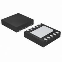
IC CTLR SYNC BUCK 1PH LV 10-DFN
Manufacturer
ON Semiconductor
Type
Step-Down (Buck)r
Datasheet
1.NCP1589BMNTXG.pdf
(10 pages)
Specifications of NCP1589AMNTWG
Internal Switch(s)
No
Synchronous Rectifier
Yes
Number Of Outputs
1
Voltage - Output
Adj to 0.8V
Current - Output
1.5A
Frequency - Switching
300kHz
Voltage - Input
4.5 ~ 13.2 V
Operating Temperature
0°C ~ 70°C
Mounting Type
Surface Mount
Package / Case
10-VFDFN Exposed Pad
Topology
Boost, Buck
Output Voltage
0.4 V
Output Current
8 mA
Switching Frequency
300 KHz
Duty Cycle (max)
80 %
Operating Supply Voltage
15 V
Supply Current
8 mA
Maximum Operating Temperature
+ 150 C
Minimum Operating Temperature
0 C
Mounting Style
SMD/SMT
Lead Free Status / RoHS Status
Lead free / RoHS Compliant
Power - Output
-
Available stocks
Company
Part Number
Manufacturer
Quantity
Price
Company:

Part Number:
NCP1589AMNTWG
Manufacturer:
ON Semiconductor
Quantity:
3 000
Company:
Part Number:
NCP1589AMNTWG
Manufacturer:
ON Semiconductor
Quantity:
500
Part Number:
NCP1589AMNTWG
Manufacturer:
ON/安森美
Quantity:
20 000


Stresses exceeding Maximum Ratings may damage the device. Maximum Ratings are stress ratings only. Functional operation above the
Recommended Operating Conditions is not implied. Extended exposure to stresses above the Recommended Operating Conditions may affect
device reliability.
This device is ESD sensitive. Use standard ESD precautions when handling.
PIN FUNCTION DESCRIPTION
Pin No.
ABSOLUTE MAXIMUM RATINGS
MAXIMUM RATINGS
Thermal Resistance, Junction−to−Ambient
Thermal Resistance, Junction−to−Case
Operating Junction Temperature Range
Operating Ambient Temperature Range
Storage Temperature Range
Moisture Sensitivity Level
Main Supply Voltage Input
Bootstrap Supply Voltage Input
Switching Node (Bootstrap Supply Return)
High−Side Driver Output (Top Gate)
Low−Side Driver Output (Bottom Gate)
Feedback, VOS
COMP/EN
PGOOD
10
1
2
3
4
5
6
7
8
9
COMP/EN
PGOOD
Symbol
BOOT
GND
VCC
VOS
UG
LG
LX
FB
Supply rail for the floating top gate driver. To form a boost circuit, use an external diode to bring the desired
input voltage to this pin (cathode connected to BOOT pin). Connect a capacitor (C
the LX pin. Typical values for C
Switch node pin. This is the reference for the floating top gate driver. Connect this pin to the source of the top
MOSFET.
Top gate MOSFET driver pin. Connect this pin to the gate of the top N−channel MOSFET.
Bottom gate MOSFET driver pin. Connect this pin to the gate of the bottom N−channel MOSFET.
IC ground reference. All control circuits are referenced to this pin.
Supply rail for the internal circuitry. Operating supply range is 4.5 V to 13.2 V. Decouple with a 1 mF capacitor
to GND. Ensure that this decoupling capacitor is placed near the IC.
Compensation Pin. This is the output of the error amplifier (EA) and the non−inverting input of the PWM com-
parator. Use this pin in conjunction with the FB pin to compensate the voltage−control feedback loop. Pull this
pin low for disable.
This pin is the inverting input to the error amplifier. Use this pin in conjunction with the COMP pin to com-
pensate the voltage−control feedback loop. Connect this pin to the output resistor divider (if used) or directly
to V
Voltage Offset Sense
Power Good output. Pulled Low if VOS is ±10% of 0.8 V V
Pin Name
out
Rating
.
BOOT
http://onsemi.com
range from 0.1 mF to 1 mF. Ensure that C
3
COMP/EN
Description
FB, VOS
PGOOD
Symbol
Symbol
BOOT
VCC
R
R
MSL
T
UG
LG
LX
T
T
qJC
qJA
stg
A
J
ref
.
40 V for < 100 ns
40 V for < 100 ns
35 V wrt/GND
40 V < 100 ns
30 V wrt/GND
V
−55 to +150
15 V wrt/LX
15 V wrt/LX
CC
0 to 150
0 to 70
Value
V
5.0 V
3.6 V
15 V
35 V
165
7 V
MAX
45
+ 0.3 V
1
BOOT
BOOT
is placed near the IC.
) between this pin and
−10 V for < 200 ns
−2 V for < 200 ns
−5 V for < 200 ns
−0.3 V wrt/LX
−0.3 V
−0.3 V
−0.3 V
−0.3 V
−0.3 V
−0.3 V
−0.3 V
−0.3 V
°C/W
°C/W
V
−5 V
Unit
°C
°C
°C
MIN
−
Related parts for NCP1589AMNTWG
Image
Part Number
Description
Manufacturer
Datasheet
Request
R

Part Number:
Description:
Low Voltage Synchronous Buck Controller
Manufacturer:
ON Semiconductor
Datasheet:

Part Number:
Description:
THERMISTOR 100K OHM NTC 0402 SMD
Manufacturer:
Murata Electronics North America
Datasheet:
Part Number:
Description:
THERMISTOR 100K OHM NTC 0402 SMD
Manufacturer:
Murata Electronics North America
Datasheet:
Part Number:
Description:
THERMISTOR 68K OHM NTC 0402 SMD
Manufacturer:
Murata Electronics North America
Datasheet:
Part Number:
Description:
THERMISTOR 10K OHM NTC 0402 SMD
Manufacturer:
Murata Electronics North America
Datasheet:
Part Number:
Description:
THERMISTOR 47K OHM NTC 0402 SMD
Manufacturer:
Murata Electronics North America
Datasheet:
Part Number:
Description:
THERMISTOR 4.7K OHM NTC 0402 SMD
Manufacturer:
Murata Electronics North America
Datasheet:
Part Number:
Description:
THERMISTOR 47K OHM NTC 0402 SMD
Manufacturer:
Murata Electronics North America
Datasheet:
Part Number:
Description:
THERMISTOR 10K OHM NTC 0402 SMD
Manufacturer:
Murata Electronics North America
Datasheet:
Part Number:
Description:
THERMISTOR 470K OHM NTC 0402 SMD
Manufacturer:
Murata Electronics North America
Datasheet:
Part Number:
Description:
THERMISTOR 22K OHM NTC 0402 SMD
Manufacturer:
Murata Electronics North America
Datasheet:
Part Number:
Description:
THERMISTOR 220K OHM NTC 0402 SMD
Manufacturer:
Murata Electronics North America
Datasheet:
Part Number:
Description:
THERMISTOR 150 OHM NTC 0402 SMD
Manufacturer:
Murata Electronics North America
Datasheet:
Part Number:
Description:
THERMISTOR 15K OHM NTC 0402 SMD
Manufacturer:
Murata Electronics North America
Datasheet:
Part Number:
Description:
THERMISTOR 150K OHM NTC 0402 SMD
Manufacturer:
Murata Electronics North America
Datasheet: