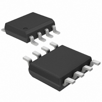
MAX619CSA Maxim Integrated Products, MAX619CSA Datasheet - Page 4

MAX619CSA
Manufacturer Part Number
MAX619CSA
Description
IC DC/DC CONV CHRG PUMP 5V 8SOIC
Manufacturer
Maxim Integrated Products
Type
Switched Capacitor (Charge Pump)r
Datasheet
1.MAX619CSA.pdf
(7 pages)
Specifications of MAX619CSA
Internal Switch(s)
Yes
Synchronous Rectifier
No
Number Of Outputs
1
Voltage - Output
5V
Current - Output
50mA
Frequency - Switching
500kHz
Voltage - Input
2 ~ 3.6 V
Operating Temperature
0°C ~ 70°C
Mounting Type
Surface Mount
Package / Case
8-SOIC (3.9mm Width)
Power - Output
471mW
Function
Step Up
Output Voltage
5 V
Output Current
50 mA
Maximum Operating Temperature
+ 70 C
Minimum Operating Temperature
0 C
Mounting Style
SMD/SMT
Lead Free Status / RoHS Status
Contains lead / RoHS non-compliant
Other names
Q1143368A
Available stocks
Company
Part Number
Manufacturer
Quantity
Price
Company:
Part Number:
MAX619CSA
Manufacturer:
MAXIM
Quantity:
10
Company:
Part Number:
MAX619CSA
Manufacturer:
MAXIM
Quantity:
15
Part Number:
MAX619CSA
Manufacturer:
MAXIM/美信
Quantity:
20 000
Part Number:
MAX619CSA+T
Manufacturer:
MAXIM/美信
Quantity:
20 000
_____________________Pin Description
Regulated 5V Charge-Pump
DC-DC Converter
PIN
The MAX619 provides a regulated 5V output from a 2V
to 3.6V (two battery cells) input. Internal charge pumps
and external capacitors generate the 5V output, elimi-
nating the need for inductors. The output voltage is
regulated to 5V ±4% by a pulse-skipping controller that
turns on the charge pump when the output voltage
begins to droop.
To maintain the greatest efficiency over the entire input
voltage range, the MAX619’s internal charge pump
operates as a voltage doubler when V
3.0V to 3.6V, and as a voltage tripler when V
from 2.0V to 2.5V. When V
4
_______________Detailed Description
1
2
3
4
5
6
7
8
________________________________________________________________________________________
NAME
SHDN
GND
C1+
OUT
C2+
C2-
C1-
IN
Positive Terminal for C1
Input Supply Voltage
+5V Output Voltage. V
shutdown mode.
Positive Terminal for C2
Negative Terminal for C2
Ground
Active-High CMOS Logic-Level Shutdown Input
Negative Terminal for C1
IN
FUNCTION
ranges from 2.5V to 3.0V,
Operating Principle
OUT
= 0V when in
IN
ranges from
IN
ranges
the MAX619 switches between doubler and tripler
mode on alternating cycles, making a 2.5 x V
pump. To further enhance efficiency over the input
range, an internal comparator selects the higher of V
or V
Efficiency with V
80%.
Figure 1 shows a detailed block diagram of the
MAX619. In tripler mode, when the S1 switches close,
the S2 switches open and capacitors C1 and C2
charge up to V
and C2 are connected in series between IN and OUT
when the S1 switches open and the S2 switches close,
as shown in Figure 1. In doubler mode, only C2 is
used.
During one oscillator cycle, energy is transferred from
the input to the charge-pump capacitors, and then
from the charge-pump capacitors to the output capaci-
tor and load. The number of cycles within a given time
frame increases as the load increases or as the input
supply voltage decreases. In the limiting case, the
charge pumps operate continuously, and the oscillator
frequency is nominally 500kHz.
The MAX619 enters low-power shutdown mode when
SHDN is a logic high. SHDN is a CMOS-compatible
input. In shutdown mode, the charge-pump switching
action is halted, OUT is disconnected from IN, and
V
operation. When V
5V in 0.5ms under no-load conditions after SHDN goes
low.
OUT
OUT
falls to 0V. Connect SHDN to ground for normal
to run the MAX619’s internal circuitry.
IN
IN
. On the second half of the cycle, C1
= 2V and I
IN
= 3.6V, V
OUT
OUT
Shutdown Mode
= 20mA is typically
typically reaches
IN
charge
IN


