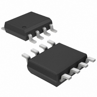
MAX619CSA Maxim Integrated Products, MAX619CSA Datasheet - Page 7

MAX619CSA
Manufacturer Part Number
MAX619CSA
Description
IC DC/DC CONV CHRG PUMP 5V 8SOIC
Manufacturer
Maxim Integrated Products
Type
Switched Capacitor (Charge Pump)r
Datasheet
1.MAX619CSA.pdf
(7 pages)
Specifications of MAX619CSA
Internal Switch(s)
Yes
Synchronous Rectifier
No
Number Of Outputs
1
Voltage - Output
5V
Current - Output
50mA
Frequency - Switching
500kHz
Voltage - Input
2 ~ 3.6 V
Operating Temperature
0°C ~ 70°C
Mounting Type
Surface Mount
Package / Case
8-SOIC (3.9mm Width)
Power - Output
471mW
Function
Step Up
Output Voltage
5 V
Output Current
50 mA
Maximum Operating Temperature
+ 70 C
Minimum Operating Temperature
0 C
Mounting Style
SMD/SMT
Lead Free Status / RoHS Status
Contains lead / RoHS non-compliant
Other names
Q1143368A
Available stocks
Company
Part Number
Manufacturer
Quantity
Price
Company:
Part Number:
MAX619CSA
Manufacturer:
MAXIM
Quantity:
10
Company:
Part Number:
MAX619CSA
Manufacturer:
MAXIM
Quantity:
15
Part Number:
MAX619CSA
Manufacturer:
MAXIM/美信
Quantity:
20 000
Part Number:
MAX619CSA+T
Manufacturer:
MAXIM/美信
Quantity:
20 000
The MAX619’s high oscillator frequency makes good
layout important. A good layout ensures stability and
helps maintain the output voltage under heavy loads.
For best performance, use very short connections to
the capacitors.
Two MAX619s can be placed in parallel to increase
output drive capability. The IN, OUT, and GND pins
can be paralleled, but C1 and C2 pins cannot.
input bypass capacitor and output filter capacitor are,
to some extent, shared when two circuits are paral-
leled. If the circuits are physically close together, it
may be possible to use a single bypass and a single
output capacitor, each with twice the value of the single
circuit. If the MAX619s cannot be placed close togeth-
er, use separate bypass and output capacitors. The
amount of output ripple observed will determine
whether single input bypass and output filter capacitors
can be used.
Figure 3. Paralleling Two MAX619s
INPUT
________________________________________________________________________________________
IN
IN
MAX619
MAX619
GND
GND
Layout Considerations
OUT
OUT
Paralleling Devices
5V, 40mA
Regulated 5V Charge-Pump
The
___________________Chip Topography
TRANSISTOR COUNT: 599;
SUBSTRATE CONNECTED TO GND.
OUT
C2+
IN
DC-DC Converter
C1+
(1.828mm)
0.072”
C1-
C2-
GND
SHDN
(2.921mm)
0.115”
7


