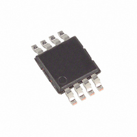
MAX1674EUA+T Maxim Integrated Products, MAX1674EUA+T Datasheet - Page 8

MAX1674EUA+T
Manufacturer Part Number
MAX1674EUA+T
Description
IC DC-DC CONV HI EFF 8-UMAX
Manufacturer
Maxim Integrated Products
Type
Step-Up (Boost)r
Datasheet
1.MAX1674EUA.pdf
(12 pages)
Specifications of MAX1674EUA+T
Internal Switch(s)
Yes
Synchronous Rectifier
Yes
Number Of Outputs
1
Voltage - Output
3.3V, 5V, Adj
Current - Output
420mA
Frequency - Switching
500kHz
Voltage - Input
0.7 ~ 5.5 V
Operating Temperature
-40°C ~ 85°C
Mounting Type
Surface Mount
Package / Case
8-MSOP, Micro8™, 8-uMAX, 8-uSOP,
Power - Output
330mW
Lead Free Status / RoHS Status
Lead free / RoHS Compliant
As a result, the synchronous rectifier significantly
improves efficiency without the addition of an external
component. Conversion efficiency can be as high as
94%, as shown in the Typical Operating Characteristics.
For low-voltage inputs from single cells (Alkaline, NiCd,
or NiMH), use an external Schottky diode such as the
1N5817 to ensure start-up.
The voltage at REF is nominally +1.30V. REF can
source up to 100µA to external circuits. The reference
maintains excellent load regulation (see Typical Oper-
ating Characteristics). A bypass capacitor of 0.1µF is
required for proper operation.
The device enters shutdown when V
(V
SHDN high (V
to OUT. During shutdown, the body diode of the P-
channel MOSFET allows current flow from the battery to
the output. V
LX remains high impedance. The capacitance and load
at OUT determine the rate at which V
Shutdown can be pulled as high as 6V, regardless of
the voltage at OUT.
The MAX1676 allows a selectable inductor current limit
of either 0.5A or 1A. This allows flexibility in designing
for higher current applications or for smaller, compact
designs. Connect CLSEL to OUT for 1A or to GND for
0.5A. CLSEL draws 1.4µA when connected to OUT.
The MAX1676 is designed with an internal damping
switch to minimize ringing at LX. The damping switch
connects an external resistor (R1) across the inductor
when the inductor’s energy is depleted (Figure 2).
Normally, when the energy in the inductor is insufficient
to supply current to the output, the capacitance and
inductance at LX form a resonant circuit that causes
ringing. The ringing continues until the energy is dissi-
pated through the series resistance of the inductor. The
damping switch supplies a path to quickly dissipate this
energy, minimizing the ringing at LX. Damping LX ring-
ing does not reduce V
R1 = 200Ω works well for most applications while reduc-
ing efficiency by only 1%. Larger R1 values provide less
damping, but have less impact on efficiency. Generally,
lower values of R1 are needed to fully damp LX when
the V
High-Efficiency, Low-Supply-Current,
Compact, Step-Up DC-DC Converters
8
SHDN
_______________________________________________________________________________________
OUT
<20% of V
/V
Current Limit Select Pin (MAX1676)
IN
BATT/Damping Switch (MAX1676)
OUT
ratio is high (Figures 2, 3, and 4).
SHDN
falls to approximately V
OUT
>80% of V
OUT
). For normal operation, drive
ripple, but does reduce EMI.
Voltage Reference
OUT
) or connect SHDN
IN
OUT
SHDN
Shutdown
- 0.6V and
decays.
is low
Figure 2. Simplified Diagram of Inductor Damping Switch
Figure 4. LX Waveform with Damping Switch (with 200Ω
external resistor)
Figure 3. LX Ringing Without Damping Switch
MAX1676
BATT
DAMPING
SWITCH
R1
200Ω
2µs/div
2µs/div
OUT
LX
0.1µF
V
IN
22µH
47µF
V
OUT
V
1V/div
V
1V/div
LX
LX


