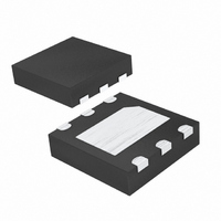
MAX1836ETT50+T Maxim Integrated Products, MAX1836ETT50+T Datasheet - Page 10

MAX1836ETT50+T
Manufacturer Part Number
MAX1836ETT50+T
Description
IC DC-DC CONV 5V 6-TDFN
Manufacturer
Maxim Integrated Products
Type
Step-Down (Buck)r
Datasheet
1.MAX1837ETT50T.pdf
(15 pages)
Specifications of MAX1836ETT50+T
Internal Switch(s)
Yes
Synchronous Rectifier
No
Number Of Outputs
1
Voltage - Output
4.8 ~ 5.2 V
Current - Output
125mA
Voltage - Input
4.5 ~ 24 V
Operating Temperature
-40°C ~ 85°C
Mounting Type
Surface Mount
Package / Case
6-TDFN Exposed Pad
Power - Output
1.95W
Lead Free Status / RoHS Status
Lead free / RoHS Compliant
Frequency - Switching
-
Lead Free Status / Rohs Status
Lead free / RoHS Compliant
24V Internal Switch, 100% Duty Cycle,
Step-Down Converters
The inductor’s saturation current rating must be greater
than the peak switching current, which is determined
by the switch current limit plus the overshoot due to the
300ns current-sense comparator propagation delay:
where the switch current-limit (I
(MAX1836) or 625mA (MAX1837). Saturation occurs
when the inductor’s magnetic flux density reaches the
maximum level the core can support, and the induc-
tance starts to fall.
Inductor series resistance affects both efficiency and
dropout voltage (see the Input-Output Voltage section).
High series resistance limits the maximum current avail-
able at lower input voltages and increases the dropout
voltage. For optimum performance, select an inductor
with the lowest possible DC resistance that fits in the
allotted dimensions. Typically, the inductor’s series resis-
tance should be significantly less than that of the internal
P-channel MOSFET’s on-resistance (1.1Ω typ). Inductors
with a ferrite core, or equivalent, are recommended.
The maximum output current of the MAX1836/MAX1837
current-limited converter is limited by the peak inductor
current. For the typical application, the maximum out-
put current is approximately:
Choose the output capacitor to supply the maximum
load current with acceptable voltage ripple. The output
ripple has two components: variations in the charge
stored in the output capacitor with each LX pulse, and
the voltage drop across the capacitor’s equivalent
series resistance (ESR) caused by the current into and
out of the capacitor:
The output voltage ripple as a consequence of the ESR
and output capacitance is:
where I
Inductor Selection section). These equations are suit-
able for initial capacitor selection, but final values
10
______________________________________________________________________________________
V
V
RIPPLE(ESR)
RIPPLE(C)
PEAK
V
I
PEAK
RIPPLE
is the peak inductor current (see the
=
=
I
≈
LIM
I
OUT(MAX)
L I
=
V
(
2C
RIPPLE(ESR)
I
PEAK
PEAK
+
(V - V
OUT OUT
IN
ESR
- I
V
=
OUT
OUT
1
2
LIM
L
I
Output Capacitor
+
PEAK
)
2
)
V
) is typically 312mA
⎛
⎜
⎝
RIPPLE(C)
300
V - V
IN
ns
V
IN
OUT
⎞
⎟
⎠
should be set by testing a prototype or evaluation cir-
cuit. As a general rule, a smaller amount of charge
delivered in each pulse results in less output ripple.
Since the amount of charge delivered in each oscillator
pulse is determined by the inductor value and input
voltage, the voltage ripple increases with larger induc-
tance but decreases with lower input voltages.
With low-cost aluminum electrolytic capacitors, the
ESR-induced ripple can be larger than that caused by
the current into and out of the capacitor. Consequently,
high-quality low-ESR aluminum-electrolytic, tantalum,
polymer, or ceramic filter capacitors are required to
minimize output ripple. Best results at reasonable cost
are typically achieved with an aluminum-electrolytic
capacitor in the 100µF range, in parallel with a 0.1µF
ceramic capacitor.
The input filter capacitor reduces peak currents drawn
from the power source and reduces noise and voltage
ripple on the input caused by the circuit’s switching.
The input capacitor must meet the ripple-current
requirement (I
defined by the following equation:
For most applications, nontantalum chemistries (ceram-
ic, aluminum, polymer, or OS-CON) are preferred due to
their robustness with high inrush currents typical of sys-
tems with low-impedance battery inputs. Alternatively,
two (or more) smaller-value low-ESR capacitors can be
connected in parallel for lower cost. Choose an input
capacitor that exhibits <+10°C temperature rise at the
RMS input current for optimal circuit longevity.
The current in the external diode (D1) changes abruptly
from zero to its peak value each time the LX switch
turns off. To avoid excessive losses, the diode must
have a fast turn-on time and a low forward voltage. Use
a diode with an RMS current rating of 0.5A or greater,
and with a breakdown voltage >V
are preferred. For high-temperature applications,
Schottky diodes may be inadequate due to their high
leakage currents. In such cases, ultra-high-speed sili-
con rectifiers are recommended, although a Schottky
diode with a higher reverse voltage rating can often
provide acceptable performance.
I
RMS
RMS
=
I
LOAD
) imposed by the switching currents
V
OUT
(
V - V
V
IN
IN
Diode Selection
Input Capacitor
IN
OUT
. Schottky diodes
)


