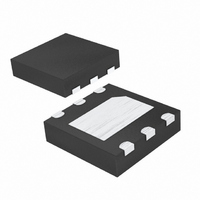
MAX1836ETT50+T Maxim Integrated Products, MAX1836ETT50+T Datasheet - Page 9

MAX1836ETT50+T
Manufacturer Part Number
MAX1836ETT50+T
Description
IC DC-DC CONV 5V 6-TDFN
Manufacturer
Maxim Integrated Products
Type
Step-Down (Buck)r
Datasheet
1.MAX1837ETT50T.pdf
(15 pages)
Specifications of MAX1836ETT50+T
Internal Switch(s)
Yes
Synchronous Rectifier
No
Number Of Outputs
1
Voltage - Output
4.8 ~ 5.2 V
Current - Output
125mA
Voltage - Input
4.5 ~ 24 V
Operating Temperature
-40°C ~ 85°C
Mounting Type
Surface Mount
Package / Case
6-TDFN Exposed Pad
Power - Output
1.95W
Lead Free Status / RoHS Status
Lead free / RoHS Compliant
Frequency - Switching
-
Lead Free Status / Rohs Status
Lead free / RoHS Compliant
A step-down converter’s minimum input-to-output volt-
age differential (dropout voltage) determines the lowest
useable input supply voltage. In battery-powered sys-
tems, this limits the useful end-of-life battery voltage. To
maximize battery life, the MAX1836/MAX1837 operate
with duty cycles up to 100%, which minimizes the input-
to-output voltage differential. When the supply voltage
approaches the output voltage, the P-channel MOSFET
remains on continuously to supply the load.
Dropout voltage is defined as the difference between
the input and output voltages when the input is low
enough for the output to drop out of regulation. For a
step-down converter with 100% duty cycle, the dropout
voltage depends on the MOSFET drain-to-source on-
resistance (R
therefore, it is proportional to the load current:
A logic-level low voltage on SHDN shuts down the
MAX1836/MAX1837. When shut down, the supply current
drops to 3µA to maximize battery life, and the internal P-
channel MOSFET turns off to isolate the output from the
input. The output capacitance and load current determine
the rate at which the output voltage decays. A logic-level
high voltage on SHDN activates the MAX1836/MAX1837.
Do not leave SHDN floating. If unused, connect SHDN to
IN. When setting output voltages above 5.5V, the shut-
down feature cannot be used, so SHDN must be perma-
nently connected to IN. The SHDN input voltage slew rate
must be greater than 10V/ms.
Thermal-overload protection limits total power dissipa-
tion in the MAX1836/MAX1837. When the junction tem-
perature exceeds T
off the pass transistor, allowing the IC to cool. The ther-
mal sensor turns the pass transistor on again after the
IC’s junction temperature cools by 10°C, resulting in
a pulsed output during continuous thermal-overload
conditions.
The feedback input features dual-mode operation.
Connect the output to OUT and FB to GND for the pre-
set output voltage. The MAX1836/MAX1837 are sup-
plied with factory-set output voltages of 3.3V or 5V. The
two-digit part number suffix identifies the output voltage
V
DROPOUT
DS(ON)
Input-Output (Dropout) Voltage
=
Thermal-Overload Protection
_______________________________________________________________________________________
I
OUT
J
) and inductor series resistance;
= +160°C, a thermal sensor turns
24V Internal Switch, 100% Duty Cycle,
Output Voltage Selection
×
Design Information
(
R
DS(ON)
Shutdown ( SHDN )
+
R
INDUCTOR
)
(see the Selector Guide). For example, the
MAX1836EUT33 has a preset 3.3V output voltage.
The MAX1836/MAX1837 output voltage may be adjust-
ed by connecting a voltage divider from the output to
FB (Figure 5). When externally adjusting the output volt-
age, connect OUT to GND. Select R2 in the 10kΩ to
100kΩ range. Calculate R1 with the following equation:
where V
V
down feature cannot be used, so SHDN must be per-
manently connected to IN.
When selecting the inductor, consider these four para-
meters: inductance value, saturation current rating,
series resistance, and size. The MAX1836/MAX1837
operate with a wide range of inductance values. For
most applications, values between 10µH and 100µH
work best with the controller’s switching frequency.
Calculate the minimum inductance value as follows:
where t
L
smaller in physical size and less expensive, but they
result in higher peak-current overshoot due to current-
sense comparator propagation delay (300ns). Peak-
current overshoot reduces efficiency and could exceed
the current ratings of the internal switching MOSFET
and external components.
Figure 5. Adjustable Output Voltage
Step-Down Converters
IN
(MIN)
NOTE: HIGH-CURRENT PATHS SHOWN WITH BOLD LINES.
. When setting output voltages above 5.5V, the shut-
INPUT
4.5V OR 24V
C
IN
ON(MIN)
are acceptable. Low-value inductors may be
FB
L
= 1.25V, and V
(MIN)
IN
GND
SHDN
= 1.0µs. Inductor values up to six times
=
R1 R2
(V
=
MAX1836
MAX1837
IN(MAX)
⎡
⎢
⎢
⎣
⎛
⎜
⎝
OUT
V
V
OUT
OUT
- V
LX
FB
FB
I
LIM
OUT ON(MIN)
may range from 1.25V to
Inductor Selection
⎞
⎟
⎠
-
)
1
t
⎤
⎥
⎥
⎦
D1
L1
R1
R2
1.25V TO V
OUTPUT
C
IN
OUT
9


