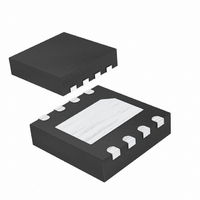
MAX15032ATA+T Maxim Integrated Products, MAX15032ATA+T Datasheet - Page 8

MAX15032ATA+T
Manufacturer Part Number
MAX15032ATA+T
Description
IC DC-DC CONV STEP-UP 8-TDFN
Manufacturer
Maxim Integrated Products
Type
Step-Up (Boost)r
Datasheet
1.MAX15032ATAT.pdf
(10 pages)
Specifications of MAX15032ATA+T
Internal Switch(s)
Yes
Synchronous Rectifier
No
Number Of Outputs
1
Voltage - Output
6.6 ~ 36 V
Current - Output
1A
Frequency - Switching
500kHz
Voltage - Input
2.7 ~ 11 V
Operating Temperature
-40°C ~ 125°C
Mounting Type
Surface Mount
Package / Case
8-TDFN Exposed Pad
Power - Output
1.95W
Lead Free Status / RoHS Status
Lead free / RoHS Compliant
500kHz, 36V Output, 600mW PWM
Step-Up DC-DC Converter
If the boost converter remains in the discontinuous
mode of operation, then the approximate peak inductor
current, I
below:
where T
volts, V
is the output current in amperes, L is the inductor value in
µH, and η is the efficiency of the boost converter.
Three key inductor parameters must be specified for
operation with the MAX15032: inductance value (L),
inductor saturation current (I
tance (DCR). In general, the inductor should have a
saturation current rating greater than the maximum
switch peak current-limit value (I
DCR should be below 0.1Ω for reasonable efficiency.
Due to the high switching frequency of the MAX15032,
inductors with a ferrite core or equivalent are recom-
mended to minimize core losses. Table 1 shows a list of
vendors with 4.7µH inductor parts.
Table 1. Inductor Vendors
Use the following formula to calculate the lower bound
of the inductor value at different output voltages and
output currents. This is the minimum inductance value
for discontinuous mode operation for supplying the full
600mW output power:
where V
ues, T
I
8
TDK
TOKO
Coilcraft
LIM-LX
VENDOR
_______________________________________________________________________________________
L
I
LPEAK
MIN
S
IN_MIN
is the peak LX current (A).
S
IN
(µs) is the period, η is the efficiency, and
is the period in µs, V
LPEAK
[
Determining Peak Inductor Current
408-437-9585 408-437-9591
847-297-0070 847-699-7864 636CY-4R7M+P3
800-322-2645 847-639-1469 MOS6020-472MLC
μ
(V), V
H
=
PHONE
]
is the minimum input voltage in volts, I
Determining the Inductor Value
=
2
OUT
2
(A), is represented by the formula
×
×
T
T
S
S
(V), and I
×
×
(
I
V
OUT
OUT
η
FAX
SAT
OUT
×
η
I
×
2
OUT
−
×
), and DC series resis-
(
LIM LX
V
V
is the output voltage in
L
LIM-LX(MAX)
IN MIN
OUT
−
(A) are typical val-
_
SLF7045T-
4R7M2R0-PF
−
PART NUMBER
V
)
INDUCTOR
IN MIN
OF 4.7µH
×
I
_
OUT
= 1.7A).
)
OUT
Calculate the optimum value of L (L
the full output power without reaching the boundary
between continuous conduction mode (CCM) and DCM
using the following formula:
where:
For a design in which V
I
4.7µH:
and
For a worst-case scenario in which V
30V, I
1.8µs:
and:
The choice of 4.7µH is reasonable given the worst-case
scenario above. In general, the higher the inductance,
the lower the switching noise.
The MAX15032’s high switching frequency demands a
high-speed rectifier. Schottky diodes are recommend-
ed for most applications because of their fast recovery
time and low forward-voltage drop. Ensure that the
diode’s peak current rating is greater than the inductor
peak current. Also, the diode reverse breakdown volt-
age must be greater than V
For most applications, use a small ceramic surface-mount
output capacitor, 2.2µF or greater. To achieve low output
ripple, a capacitor with low-ESR, low-ESL, and high-
capacitance value should be selected. If tantalum or
electrolytic capacitors are used to achieve high capaci-
tance values, always add a small ceramic in parallel to
bypass the high-frequency components of the diode cur-
rent. The higher ESR and ESL of electrolytic increase both
the output ripple and peak-to-peak transient voltage.
Assuming the contribution from the ESR and capacitor
OUT
L
MAX
= 20mA, η = 0.7, and T
OUT
[
μ
= 20mA, η = 0.7, I
H
]
Output Filter Capacitor Selection
=
L
V
OPTIMUM
IN MIN
_
L
L
L
L
MAX
MAX
MIN
MIN
2
2
(
= 10.5µH
= 3.3µH
= 2.2µH
V
= 9.2µH
×
=
OUT
OUT
IN
I
LIM-LX(MIN)
L
OUT
MAX
.
= 3.3V, V
2 25
S
−
.
×
V
= 2µs, L
[
Diode Selection
IN MIN
μ
OPTIMUM
V V
H
OUT
IN
_
]
= 2.9V, V
= 1A, and T
2
)
OUT
OPTIMUM
×
) to ensure
T
S
= 30V,
×
OUT
η
S
=
=
=


