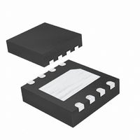
MAX15032ATA+T Maxim Integrated Products, MAX15032ATA+T Datasheet - Page 9

MAX15032ATA+T
Manufacturer Part Number
MAX15032ATA+T
Description
IC DC-DC CONV STEP-UP 8-TDFN
Manufacturer
Maxim Integrated Products
Type
Step-Up (Boost)r
Datasheet
1.MAX15032ATAT.pdf
(10 pages)
Specifications of MAX15032ATA+T
Internal Switch(s)
Yes
Synchronous Rectifier
No
Number Of Outputs
1
Voltage - Output
6.6 ~ 36 V
Current - Output
1A
Frequency - Switching
500kHz
Voltage - Input
2.7 ~ 11 V
Operating Temperature
-40°C ~ 125°C
Mounting Type
Surface Mount
Package / Case
8-TDFN Exposed Pad
Power - Output
1.95W
Lead Free Status / RoHS Status
Lead free / RoHS Compliant
discharge equals 50% (proportions could vary), calcu-
late the output capacitance and ESR required for a spec-
ified ripple using the following equations:
For very low output-ripple applications, the output of the
boost converter can be followed by an RC filter to fur-
ther reduce the ripple. Figure 1 shows a 10Ω, 2.2µF fil-
ter used to reduce the switching output ripple to
1mV
400µV
tion resistive divider must remain connected to the
diode/output capacitor node.
X7R ceramic capacitors are stable over -40°C to
+125°C temperature range. Where the automotive tem-
perature range is required, use X7R ceramic capaci-
tors. X5R dielectric can be used for -40°C to +85°C
applications.
Bypass IN (the input voltage pin) to PGND with a mini-
mum 4.7µF ceramic capacitor. Depending on the sup-
ply source impedance, higher values might be needed.
Make sure that the input capacitor is close enough to
the IC to provide adequate decoupling at IN as well. If
the layout cannot achieve this, add another 0.1µF
ceramic capacitor between IN and PGND in the imme-
Figure 1. Typical Operating Circuit with RC Filter
C
OUT
P-P
P-P
[
μ
with a 20mA output and a ripple voltage of
F
with a 2mA load. The output voltage regula-
]
=
0 5 Δ
V
.
ESR m
IN
= 2.9V TO 5.5V
I
×
_______________________________________________________________________________________
OUT
[
V
Ω
OUT
Input Capacitor Selection
]
=
10μF
C
IN
0 5
⎡
⎢
⎢
⎣
T
.
S
×
I
OUT
−
Δ
I
500kHz, 36V Output, 600mW PWM
LPEAK
V
(
V
OUT
O
U U T
×
−
IN
SHDN
PGND
L
V
OPTIMUM
IN MIN
MAX15032
_
4.7μH
GND
L1
)
⎤
⎥
⎥
⎦
CN
CP
LX
FB
Step-Up DC-DC Converter
diate vicinity of the IC. Bulk aluminum electrolytic
capacitors might be needed to avoid chattering at low
input voltages. In the case of aluminum electrolytic
capacitors, calculate the capacitor value and ESR of
the input capacitor using the following equations:
Careful PCB layout is critical to achieve clean and sta-
ble operation. Protect sensitive analog grounds by
using a star ground configuration. Connect GND and
PGND together close to the device at the return terminal
of the output bypass capacitor. Do not connect them
together anywhere else. Keep all PCB traces as short
as possible to reduce stray capacitance, trace resis-
tance, and radiated noise. Ensure that the feedback
connection to FB is short and direct. Route high-speed
switching nodes away from the sensitive analog areas.
Avoid any coupling from LX to FB node by keeping the
FB node away from the LX routing. In addition, decou-
pling LX and FB with a small 22pF capacitor from FB to
GND can be used. Use an internal PCB layer for GND
as an EMI shield to keep radiated noise away from the
device, feedback dividers, and bypass capacitors.
C
10nF
C
CP
1A/40V
IN
D1
[
μ
F
]
=
η
×
V
R1
143kΩ
R2
6.2kΩ
IN MIN
V
ESR m
_
OUT
Applications Information
[
×
Ω
×
I
]
0 5 Δ
OUT
=
.
0 5
C
2.2μF
×
OUT
.
10Ω
×
R
V
F
IN
Δ
Layout Considerations
V
V
⎡
⎢
⎢
⎣
OUT
IN
T
S
×
−
η
×
I
LPEA
×
I
V
OUT
IN MIN
Δ
C
2.2μF
V
_
F
IN MIN
K K
×
_
V
30V
OUT
L
(
V
OPTIMUM
OUT
−
V
IN MIN
×
_
V
OUT
)
9
⎤
⎥ ⎥
⎥
⎦


