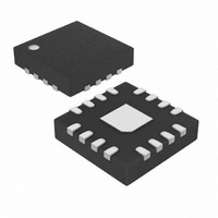
MAX8668ETEX+T Maxim Integrated Products, MAX8668ETEX+T Datasheet - Page 15

MAX8668ETEX+T
Manufacturer Part Number
MAX8668ETEX+T
Description
IC DC-DC CONV W/DUAL LDO 16TQFN
Manufacturer
Maxim Integrated Products
Type
Step-Down (Buck)r
Datasheet
1.MAX8668ETEWT.pdf
(18 pages)
Specifications of MAX8668ETEX+T
Internal Switch(s)
Yes
Synchronous Rectifier
Yes
Number Of Outputs
4
Voltage - Output
1.8V, 2.8V, 0.6 ~ 3.3 V (2)
Current - Output
600mA, 1.2A
Frequency - Switching
1.5MHz
Voltage - Input
2.6 ~ 5.5 V
Operating Temperature
-40°C ~ 85°C
Mounting Type
Surface Mount
Package / Case
16-TQFN Exposed Pad
Power - Output
1.67W
Lead Free Status / RoHS Status
Lead free / RoHS Compliant
C10 is needed if V
V
Connect a 4.7µF ceramic capacitor between OUT3 and
GND, and a second 4.7µF ceramic capacitor from
OUT4 to GND. For a constant loading above 10mA, the
output capacitors can be reduced to 2.2µF. The equiv-
alent series resistance (ESR) of the LDO output capaci-
tors affects stability and output noise. Use output
capacitors with an ESR of 0.1Ω or less to ensure stable
operation and optimum transient response. Surface-
mount ceramic capacitors have very low ESR and are
commonly available. Connect these capacitors as
close as possible to the IC’s pins to minimize PCB trace
inductance.
The maximum package power dissipation of the
MAX8667/MAX8668 is 1667mW. Make sure the power
dissipated by the MAX8667/MAX8668 does not exceed
this rating. The total IC power dissipation is the sum of
the power dissipation of the four regulators:
Estimate the OUT1 and OUT2 power dissipations as
follows:
where R
efficiency (see the Typical Operating Characteristics
section).
Calculate the OUT3 and OUT4 power dissipations as
follows:
OUT
/ 0.65.
L
is the inductor’s DC resistance, and η is the
1.5MHz Dual Step-Down DC-DC Converters
P
P
P
D
D
D
2
1
LDO Output Capacitor and Stability
=
OUT
______________________________________________________________________________________
=
=
P
I
I
OUT
D
OUT
1
with Dual LDOs and Individual Enables
> 1.5V or V
+
Thermal Considerations
2
1
P
×
×
D
2
V
V
OUT
OUT
+
P
D
1
2
3
IN12
×
×
+
1
1
P
− η
η
− η
η
D
can be less than
4
The maximum junction temperature of the MAX8667/
MAX8668 is +150°C. The junction-to-case thermal
resistance (θ
When mounted on a single-layer PCB, the junction to
ambient thermal resistance (θ
Mounted on a multilayer PCB, θ
Calculate
MAX8667/MAX8668 as follows:
where T
sure the calculated value of T
+150°C maximum.
High switching frequencies and relatively large peak
currents make PCB layout a very important aspect of
design. Good design minimizes excessive EMI on the
feedback paths and voltage gradients in the ground
plane, both of which can result in instability or regula-
tion errors. Connect the input capacitors as close as
possible to the IN_ and PGND_ pins. Connect the
inductor and output capacitors as close as possible to
the IC and keep the traces short, direct, and wide.
The feedback network traces are sensitive to inductor
magnetic field interference. Route these traces away
from the inductors and noisy traces such as LX. Keep
the feedback components close to the FB_ pin.
Connect GND and PGND_ to the ground plane.
Connect the exposed paddle to the ground plane with
one or more vias to help conduct heat away from the
IC.
Refer to the MAX8668 evaluation kit for a PCB layout
example.
A
is the maximum ambient temperature. Make
P
P
JC
the
D
D
) of the MAX8667/MAX8668 is 6.9°C/W.
3
4
=
=
I
I
OUT
junction
T
OUT
J
=
3
4
T
A
×
×
(
+
(
V
V
P
IN
IN
D
34
34
temperature
× θ
J
JA
−
−
does not exceed the
JA
JA
V
V
) is about 64°C/W.
OUT
OUT
is about 48°C/W.
3
4
PCB Layout
)
)
of
the
15


