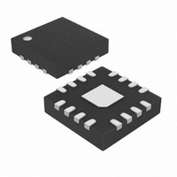
MAX8668ETEX+T Maxim Integrated Products, MAX8668ETEX+T Datasheet - Page 2

MAX8668ETEX+T
Manufacturer Part Number
MAX8668ETEX+T
Description
IC DC-DC CONV W/DUAL LDO 16TQFN
Manufacturer
Maxim Integrated Products
Type
Step-Down (Buck)r
Datasheet
1.MAX8668ETEWT.pdf
(18 pages)
Specifications of MAX8668ETEX+T
Internal Switch(s)
Yes
Synchronous Rectifier
Yes
Number Of Outputs
4
Voltage - Output
1.8V, 2.8V, 0.6 ~ 3.3 V (2)
Current - Output
600mA, 1.2A
Frequency - Switching
1.5MHz
Voltage - Input
2.6 ~ 5.5 V
Operating Temperature
-40°C ~ 85°C
Mounting Type
Surface Mount
Package / Case
16-TQFN Exposed Pad
Power - Output
1.67W
Lead Free Status / RoHS Status
Lead free / RoHS Compliant
ABSOLUTE MAXIMUM RATINGS
IN12, IN34, FB1, FB2, EN1, EN2, EN3, EN4, OUT1,
OUT3,
PGND1, PGND2 to GND .......................................-0.3V to +0.3V
LX1, LX2 Current ..........................................................1.5A RMS
LX1, LX2 to GND (Note 1) .......................-0.3V to (V IN12 + 0.3V)
1.5MHz Dual Step-Down DC-DC Converters
with Dual LDOs and Individual Enables
Note 1: LX_ has internal clamp diodes to GND and IN12. Applications that forward bias these diodes should take care not to exceed
Stresses beyond those listed under “Absolute Maximum Ratings” may cause permanent damage to the device. These are stress ratings only, and functional
operation of the device at these or any other conditions beyond those indicated in the operational sections of the specifications is not implied. Exposure to
absolute maximum rating conditions for extended periods may affect device reliability.
ELECTRICAL CHARACTERISTICS
(V
2
IN34 Supply Range
IN12 Supply Range
IN12 Suppy Range
Shutdown Supply Current,
I
No Load Supply Current,
I
UNDERVOLTAGE LOCKOUT
IN12 UVLO
IN34 UVLO
THERMAL SHUTDOWN
Threshold
Hysteresis
REFERENCE
Reference Bypass Output
Voltage
REF Supply Rejection
LOGIC AND CONTROL INPUTS
EN_ Input Low Level
EN_ Input High Level
EN_ Input Leakage Current
STEP-DOWN CONVERTERS
Minimum Adjustable Output
Voltage
IN12
IN12
IN34
OUT2, REF to GND............................................-0.3V to +6.0V
OUT4 to GND.....-0.3V to the lesser of + 6V or (V IN34 + 0.3V)
_______________________________________________________________________________________
+ I
+ I
= V
the IC’s package-dissipation limits.
IN34
IN34
IN12
PARAMETER
= 3.6V, T
A
= -40°C to +85°C, unless otherwise noted. Typical values are at T
V
MAX8668, V
MAX8667, V
V
MAX8667ETEJS+, all regulators enabled
V
V
V
V
T
2.6V ≤ (V
1.7V ≤ V
2.6V ≤ V
1.7V ≤ V
2.6V ≤ V
V
MAX8668
A
IN12
IN12
IN12
IN12
IN34
IN34
IN12
rising
≥ V
= V
rising
hysteresis
rising
hysteresis
= V
IN34
IN12
IN34
IN12
IN12
IN34
IN34
IN34
IN12
IN12
≤ 5.5V
≤ 5.5V
≤ 5.5V
≤ 5.5V
= V
= 4.2V V
= 5.5V
≥ V
≥ V
IN34
IN34
IN34
) ≤ 5.5V
CONDITIONS
EN_
= 0V
Continuous Power Dissipation (T A = +70°C)
Operating Temperature Range ...........................-40°C to +85°C
Junction Temperature ..................................................... +150°C
Storage Temperature Range .............................-65°C to +150°C
Lead Temperature (soldering, 10s) .................................+300°C
16-Pin, 3mm x 3mm Thin QFN
(derate 20.8mW/°C above +70°C) .............................1667mW
T
T
T
T
A
A
A
A
= +25°C
= +85°C
= +25°C
= +85°C
A
= +25°C.) (Note 1)
0.591
MIN
1.44
1.7
2.6
2.8
2.4
1.5
-1
+160
0.600
0.001
TYP
0.05
0.15
100
2.5
0.1
1.6
0.1
0.6
15
0.609
MAX
150
5.5
5.5
5.5
2.6
1.7
0.4
+1
1
UNITS
mV/V
µA
µA
µA
°C
°C
µA
V
V
V
V
V
V
V
V
V
V
V


