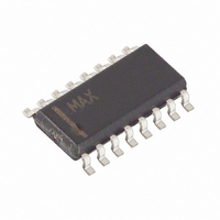
MAX1655ESE Maxim Integrated Products, MAX1655ESE Datasheet - Page 12

MAX1655ESE
Manufacturer Part Number
MAX1655ESE
Description
IC CTRLR DCDC PWM STPDWN 16-SOIC
Manufacturer
Maxim Integrated Products
Type
Step-Down (Buck)r
Datasheet
1.MAX1655ESE.pdf
(28 pages)
Specifications of MAX1655ESE
Internal Switch(s)
No
Synchronous Rectifier
Yes
Number Of Outputs
1
Voltage - Output
1 ~ 5.5 V
Current - Output
10A
Frequency - Switching
150kHz, 300kHz
Voltage - Input
4.5 ~ 30 V
Operating Temperature
-40°C ~ 85°C
Mounting Type
Surface Mount
Package / Case
16-SOIC (3.9mm Width)
Power - Output
696mW
Output Voltage
1 V to 5.5 V
Output Current
10 A
Input Voltage
4.5 V to 30 V
Mounting Style
SMD/SMT
Maximum Operating Temperature
+ 85 C
Minimum Operating Temperature
- 40 C
Lead Free Status / RoHS Status
Contains lead / RoHS non-compliant
Available stocks
Company
Part Number
Manufacturer
Quantity
Price
Company:
Part Number:
MAX1655ESE
Manufacturer:
MAXIM
Quantity:
29
Part Number:
MAX1655ESE
Manufacturer:
MAXIM/美信
Quantity:
20 000
High-Efficiency, PWM, Step-Down
DC-DC Controllers in 16-Pin QSOP
The MAX1652–MAX1655 contain nine major circuit
blocks, which are shown in Figure 2:
PWM Controller Blocks:
Bias Generator Blocks:
These internal IC blocks aren’t powered directly from
the battery. Instead, a +5V linear regulator steps down
the battery voltage to supply both the IC internal rail (VL
pin) as well as the gate drivers. The synchronous-
switch gate driver is directly powered from +5V VL,
while the high-side-switch gate driver is indirectly pow-
ered from VL via an external diode-capacitor boost cir-
cuit. An automatic bootstrap circuit turns off the +5V
linear regulator and powers the IC from its output volt-
age if the output is above 4.5V.
The heart of the current-mode PWM controller is a
multi-input open-loop comparator that sums three sig-
nals: output voltage error signal with respect to the ref-
erence voltage, current-sense signal, and slope
compensation ramp (Figure 3). The PWM controller is a
direct summing type, lacking a traditional error amplifi-
er and the phase shift associated with it. This direct-
summing configuration approaches the ideal of
cycle-by-cycle control over the output voltage.
Under heavy loads, the controller operates in full PWM
mode. Each pulse from the oscillator sets the main
PWM latch that turns on the high-side switch for a peri-
od determined by the duty factor (approximately
V
chronous rectifier latch is set. 60ns later the low-side
switch turns on, and stays on until the beginning of the
next clock cycle (in continuous mode) or until the
inductor current crosses zero (in discontinuous mode).
Under fault conditions where the inductor current
exceeds the 100mV current-limit threshold, the high-
side latch resets and the high-side switch turns off.
If the load is light in Idle Mode (SKIP = low), the induc-
tor current does not exceed the 25mV threshold set by
the Idle Mode comparator. When this occurs, the con-
troller skips most of the oscillator pulses in order to
reduce the switching frequency and cut back gate-
12
OUT
______________________________________________________________________________________
Multi-Input PWM Comparator
Current-Sense Circuit
PWM Logic Block
Dual-Mode Internal Feedback Mux
Gate-Driver Outputs
Secondary Feedback Comparator
+5V Linear Regulator
Automatic Bootstrap Switchover Circuit
+2.50V Reference
/V
IN
). As the high-side switch turns off, the syn-
PWM Controller Block
charge losses. The oscillator is effectively gated off at
light loads because the Idle Mode comparator immedi-
ately resets the high-side latch at the beginning of each
cycle, unless the feedback signal falls below the refer-
ence voltage level.
When in PWM mode, the controller operates as a fixed-
frequency current-mode controller where the duty ratio
is set by the input/output voltage ratio. The current-
mode feedback system regulates the peak inductor
current as a function of the output voltage error signal.
Since the average inductor current is nearly the same
as the peak current, the circuit acts as a switch-mode
transconductance amplifier and pushes the second out-
put LC filter pole, normally found in a duty-factor-
controlled (voltage-mode) PWM, to a higher frequency.
To preserve inner-loop stability and eliminate regenera-
tive inductor current “staircasing,” a slope-compensa-
tion ramp is summed into the main PWM comparator to
reduce the apparent duty factor to less than 50%.
The relative gains of the voltage- and current-sense
inputs are weighted by the values of current sources
that bias three differential input stages in the main PWM
comparator (Figure 4). The relative gain of the voltage
comparator to the current comparator is internally fixed
at K = 2:1. The resulting loop gain (which is relatively
low) determines the 2% typical load regulation error.
The low loop-gain value helps reduce output filter
capacitor size and cost by shifting the unity-gain
crossover to a lower frequency.
The output filter capacitor C2 sets a dominant pole in
the feedback loop. This pole must roll off the loop gain
to unity before the zero introduced by the output
capacitor’s parasitic resistance (ESR) is encountered
(see Design Procedure section). A 12kHz pole-zero
cancellation filter provides additional rolloff above the
unity-gain crossover. This internal 12kHz lowpass com-
pensation filter cancels the zero due to the filter capaci-
tor’s ESR. The 12kHz filter is included in the loop in
both fixed- and adjustable-output modes.
Synchronous rectification reduces conduction losses in
the rectifier by shunting the normal Schottky diode with
a low-resistance MOSFET switch. The synchronous rec-
tifier also ensures proper start-up of the boost-gate driv-
er circuit. If you must omit the synchronous power
MOSFET for cost or other reasons, replace it with a
small-signal MOSFET such as a 2N7002.
If the circuit is operating in continuous-conduction mode,
the DL drive waveform is simply the complement of the
DH high-side drive waveform (with controlled dead
time to prevent cross-conduction or “shoot-through”).
Synchronous-Rectifier Driver (DL Pin)


