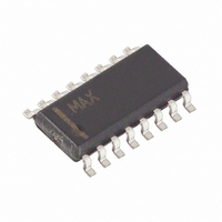
MAX1655ESE Maxim Integrated Products, MAX1655ESE Datasheet - Page 15

MAX1655ESE
Manufacturer Part Number
MAX1655ESE
Description
IC CTRLR DCDC PWM STPDWN 16-SOIC
Manufacturer
Maxim Integrated Products
Type
Step-Down (Buck)r
Datasheet
1.MAX1655ESE.pdf
(28 pages)
Specifications of MAX1655ESE
Internal Switch(s)
No
Synchronous Rectifier
Yes
Number Of Outputs
1
Voltage - Output
1 ~ 5.5 V
Current - Output
10A
Frequency - Switching
150kHz, 300kHz
Voltage - Input
4.5 ~ 30 V
Operating Temperature
-40°C ~ 85°C
Mounting Type
Surface Mount
Package / Case
16-SOIC (3.9mm Width)
Power - Output
696mW
Output Voltage
1 V to 5.5 V
Output Current
10 A
Input Voltage
4.5 V to 30 V
Mounting Style
SMD/SMT
Maximum Operating Temperature
+ 85 C
Minimum Operating Temperature
- 40 C
Lead Free Status / RoHS Status
Contains lead / RoHS non-compliant
Available stocks
Company
Part Number
Manufacturer
Quantity
Price
Company:
Part Number:
MAX1655ESE
Manufacturer:
MAXIM
Quantity:
29
Part Number:
MAX1655ESE
Manufacturer:
MAXIM/美信
Quantity:
20 000
Figure 4. Main PWM Comparator Block Diagram
In discontinuous (light-load) mode, the synchronous
switch is turned off as the inductor current falls through
zero. The synchronous rectifier works under all operat-
ing conditions, including idle mode. The synchronous-
switch timing is further controlled by the secondary
feedback (SECFB) signal in order to improve multiple-
output cross-regulation (see Secondary Feedback-
Regulation Loop section).
An internal regulator produces the 5V supply (VL) that
powers the PWM controller, logic, reference, and other
blocks. This +5V low-dropout linear regulator can sup-
ply up to 5mA for external loads, with a reserve of
20mA for gate-drive power. Bypass VL to GND with
4.7µF. Important: VL must not be allowed to exceed
5.5V. Measure VL with the main output fully loaded. If
VL is being pumped up above 5.5V, the probable
cause is either excessive boost-diode capacitance or
excessive ripple at V+. Use only small-signal diodes for
D2 (10mA to 100mA Schottky or 1N4148 are preferred)
and bypass V+ to PGND with 0.1µF directly at the
package pins.
The 2.5V reference (REF) is accurate to ±1.6% over
temperature, making REF useful as a precision system
reference. Bypass REF to GND with 0.33µF minimum.
REF can supply up to 1mA for external loads. However,
if tight-accuracy specs for either V
essential, avoid loading REF with more than 100µA.
Loading REF reduces the main output voltage slightly,
according to the reference-voltage load regulation
error. In MAX1654 applications, ensure that the SECFB
divider doesn’t load REF heavily.
Internal VL and REF Supplies
______________________________________________________________________________________
SLOPE COMPENSATION
CSH
CSL
REF
FB
I1
DC-DC Controllers in 16-Pin QSOP
High-Efficiency, PWM, Step-Down
OUT
R1
or REF are
VL
I2
R2
When the main output voltage is above 4.5V, an internal
P-channel MOSFET switch connects CSL to VL while
simultaneously shutting down the VL linear regulator.
This action bootstraps the IC, powering the internal cir-
cuitry from the output voltage, rather than through a lin-
ear regulator from the battery. Bootstrapping reduces
power dissipation caused by gate-charge and quies-
cent losses by providing that power from a 90%-effi-
cient switch-mode source, rather than from a less
efficient linear regulator.
It’s often possible to achieve a bootstrap-like effect,
even for circuits that are set to V
ing VL from an external-system +5V supply. To achieve
this pseudo-bootstrap, add a Schottky diode between
the external +5V source and VL, with the cathode to the
VL side. This circuit provides a 1% to 2% efficiency
boost and also extends the minimum battery input to
less than 4V. The external source must be in the range
of 4.8V to 5.5V.
Gate-drive voltage for the high-side N-channel switch is
generated by a flying-capacitor boost circuit as shown
in Figure 5. The capacitor is alternately charged from
the VL supply and placed in parallel with the high-side
MOSFET’s gate-source terminals.
On start-up, the synchronous rectifier (low-side MOS-
FET) forces LX to 0V and charges the BST capacitor to
5V. On the second half-cycle, the PWM turns on the
high-side MOSFET by closing an internal switch
between BST and DH. This provides the necessary
enhancement voltage to turn on the high-side switch,
I3
UNCOMPENSATED
HIGH-SPEED
LEVEL TRANSLATOR
AND BUFFER
Gate-Driver Supply (BST Pin)
OUTPUT DRIVER
OUT
Boost High-Side
< 4.5V, by power-
TO PWM
LOGIC
15


