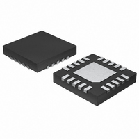
MAX1844ETP+ Maxim Integrated Products, MAX1844ETP+ Datasheet - Page 18

MAX1844ETP+
Manufacturer Part Number
MAX1844ETP+
Description
IC CNTRLR STP DWN HS 20-TQFN
Manufacturer
Maxim Integrated Products
Type
Step-Down (Buck)r
Datasheet
1.MAX1844EEP.pdf
(24 pages)
Specifications of MAX1844ETP+
Internal Switch(s)
No
Synchronous Rectifier
No
Number Of Outputs
1
Voltage - Output
1.8V, 2.5V, Adj
Current - Output
4A
Frequency - Switching
200kHz, 300kHz, 450kHz, 600kHz
Voltage - Input
2 ~ 28 V
Operating Temperature
-40°C ~ 85°C
Mounting Type
Surface Mount
Package / Case
20-TQFN Exposed Pad
Power - Output
727mW
Output Voltage
1 V to 5.5 V, 1.8 V, 2.5 V
Output Current
4000 mA
Mounting Style
SMD/SMT
Switching Frequency
600 KHz
Maximum Operating Temperature
+ 85 C
Minimum Operating Temperature
- 40 C
Synchronous Pin
No
Topology
Buck
Lead Free Status / RoHS Status
Lead free / RoHS Compliant
Stability is determined by the value of the ESR zero rela-
tive to the switching frequency. The point of instability is
given by the following equation:
where:
For a typical 300kHz application, the ESR zero frequency
must be well below 95kHz, preferably below 50kHz.
Tantalum and OS-CON capacitors in widespread use at
the time of publication have typical ESR zero frequencies
of 25kHz. In the design example used for inductor selec-
tion, the ESR needed to support 60mV
60mV/2.7A = 22mΩ. Two 470µF/4V Kemet T510 low-ESR
tantalum capacitors in parallel provide 22mΩ (max) ESR.
Their typical combined ESR results in a zero at 27kHz,
well within the bounds of stability.
Do not put high-value ceramic capacitors directly across
the feedback sense point without taking precautions to
ensure stability. Large ceramic capacitors can have a
high ESR zero frequency and cause erratic, unstable
operation. However, it’s easy to add enough series resis-
tance by placing the capacitors a couple of inches
downstream from the feedback sense point, which
should be as close as possible to the inductor.
Unstable operation manifests itself in two related but dis-
tinctly different ways: double-pulsing and fast-feedback
loop instability.
Double-pulsing occurs due to noise on the output or
because the ESR is so low that there isn’t enough volt-
age ramp in the output voltage signal. This “fools” the
error comparator into triggering a new cycle immediately
after the 400ns minimum off-time period has expired.
Double-pulsing is more annoying than harmful, resulting
in nothing worse than increased output ripple. However,
it can indicate the possible presence of loop instability,
which is caused by insufficient ESR.
Loop instability can result in oscillations at the output
after line or load perturbations that can trip the overvolt-
age protection latch or cause the output voltage to fall
below the tolerance limit.
The easiest method for checking stability is to apply a
very fast zero-to-max load transient and carefully
observe the output voltage ripple envelope for over-
shoot and ringing. It can help to monitor simultaneously
the inductor current with an AC current probe. Don’t
High-Speed Step-Down Controller with
Accurate Current Limit for Notebook Computers
18
Output Capacitor Stability Considerations
______________________________________________________________________________________
f
ESR
=
2
× ×
f
ESR
π
R
=
ESR
π
1
f
×
C
OUT
P-P
ripple is
allow more than one cycle of ringing after the initial
step-response under- or overshoot.
The input capacitor must meet the ripple current
requirement (I
Nontantalum chemistries (ceramic, aluminum, or OS-
CON) are preferred due to their resistance to power-up
surge currents.
For optimal circuit reliability, choose a capacitor that
has less than 10°C temperature rise at the peak ripple
current.
Most of the following MOSFET guidelines focus on the
challenge of obtaining high load-current capability (>5A)
when using high-voltage (>20V) AC adapters. Low-cur-
rent applications usually require less attention.
For maximum efficiency, choose a high-side MOSFET
(Q1) that has conduction losses equal to the switching
losses at the optimum battery voltage (15V). Check to
ensure that the conduction losses at minimum input
voltage do not exceed the package thermal limits or
violate the overall thermal budget. Check to ensure that
conduction losses plus switching losses at the maxi-
mum input voltage do not exceed the package ratings
or violate the overall thermal budget.
Choose a low-side MOSFET (Q2) that has the lowest
possible R
age (i.e., SO-8), and is reasonably priced. Ensure that
the MAX1844 DL gate driver can drive Q2; in other
words, check that the gate is not pulled up by the high-
side switch turn on, due to parasitic drain-to-gate capac-
itance, causing cross-conduction problems. Switching
losses are not an issue for the low-side MOSFET since it
is a zero-voltage switched device when used in the buck
topology.
Worst-case conduction losses occur at the duty factor
extremes. For the high-side MOSFET, the worst-case
power dissipation due to resistance occurs at minimum
battery voltage:
PD(Q1 Resistive) = (V
Generally, a small high-side MOSFET is desired to
reduce switching losses at high input voltages. However,
the R
DS(ON)
I
RMS
DS(ON)
required to stay within package power-dissi-
RMS
=
I
, comes in a moderate to small pack-
LOAD
) imposed by the switching currents.
MOSFET Power Dissipation
OUT
Input Capacitor Selection
Power MOSFET Selection
/ V
V
OUT
IN(MIN)
(
V - V
V
IN
IN
)
✕
I
OUT
LOAD 2
)
✕
R
DS(ON)


