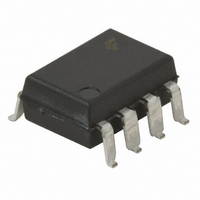
FOD2200SDV Fairchild Optoelectronics Group, FOD2200SDV Datasheet - Page 4

FOD2200SDV
Manufacturer Part Number
FOD2200SDV
Description
OPTOCOUPLER 3STATE OUTPUT 8-SOIC
Manufacturer
Fairchild Optoelectronics Group
Datasheet
1.FOD2200SDV.pdf
(11 pages)
Specifications of FOD2200SDV
Voltage - Isolation
5000Vrms
Number Of Channels
1, Unidirectional
Current - Output / Channel
25mA
Data Rate
2.5MBd
Propagation Delay High - Low @ If
180ns @ 1.6mA ~ 5mA
Current - Dc Forward (if)
5mA
Input Type
DC
Output Type
Tri-State
Mounting Type
Surface Mount
Package / Case
8-SOIC
Lead Free Status / RoHS Status
Lead free / RoHS Compliant
Other names
FOD2200SDV
FOD2200SDVTR
FOD2200SDV_NL
FOD2200SDV_NLTR
FOD2200SDV_NLTR
FOD2200SDVTR
FOD2200SDV_NL
FOD2200SDV_NLTR
FOD2200SDV_NLTR
Available stocks
Company
Part Number
Manufacturer
Quantity
Price
Company:
Part Number:
FOD2200SDV
Manufacturer:
ST
Quantity:
1 001
©2004 Fairchild Semiconductor Corporation
FOD2200 Rev. 1.0.2
Electrical Characteristics
Transfer Characteristics
V
Isolation Characteristics
*Typical values at T
Notes:
1. The V
2. t
3. t
4. When the peaking capacitor is omitted, propagation delay times may increase by 100ns.
5. t
6. t
7. CM
8. CM
9. Device considered a two-terminal device: Pins 1, 2, 3 and 4 shorted together, and Pins 5, 6, 7 and 8 shorted together.
10. Duration of output short circuit time should not exceed 10ms.
Symbol
Symbol
EL
V
R
C
I
I
I
or solid tantalum capacitor with good high frequency characteristic and should be connected as close as possible
to the package V
to the 1.3V level on the LOW to HIGH transition of the output voltage pulse.
to the 1.3V level on the HIGH to LOW transition of the output voltage pulse.
state (i.e., V
state (i.e., V
V
I
I
I
V
OHH
OSH
PLH
PHL
r
f
= 0V to 0.8V, I
OZH
OSL
HYS
I
OZL
ISO
I-O
I-O
FT
OH
OL
– Rise time is measured from the 10% to the 90% levels on the LOW to HIGH transition of the output pulse.
– Fall time is measured from the 90% to the 10% levels on the HIGH to LOW transition of the output pulse.
H
L
– Propagation delay is measured from the 50% level on the LOW to HIGH transition of the input current pulse
– Propagation delay is measured from the 50% level on the HIGH to LOW transition of the input current pulse
– The maximum tolerable rate of rise of the common mode voltage to ensure the output will remain in the low
– The maximum tolerable rate of fall of the common mode voltage to ensure the output will remain in the high
CC
Withstand Insulation Test Voltage
Resistance (Input to Output)
Capacitance (Input to Output)
Output Leakage Current
(V
Low Level Output Voltage
Input Threshold Current
Logic High Output Voltage
High Impedance State
Output Current
High Impedance State
Output Current
Logic Low Short Circuit
Output Current
Logic High Short Circuit
Output Current
Input Current Hysteresis
supply to each optoisolator must be bypassed by a 0.1µF capacitor or larger. This can be either a ceramic
OUT
DC Characteristics
OUT
OUT
F(OFF)
> V
A
> 2.0V).
< 0.8V).
Characteristics
CC
= 25°C, V
CC
and GND pins of each device.
= 0mA to 0.1mA unless otherwise specified.)
)
(10)
(10)
(T
(T
A
CC
A
= 0°C to +85°C, V
= 0°C to +85°C unless otherwise specified)
= 5V, I
(Continued)
F(ON)
V
V
I
V
I
I
V
V
V
V
V
V
V
V
V
OL
OL
OH
O
O
O
O
O
O
CC
CC
CC
CC
CC
CC
= 0.4V, V
= 2.4 V, V
= 5.5 V, V
= 20 V, V
= V
= V
= 6.4mA
= 6.4mA
= -2.6mA
= 3mA unless otherwise stated.
= 4.5V, I
= 4.5 V, I
= 4.5V, V
= 5.5V, I
= 20V, I
= 4.5V
R
V
V
CC
CC
I-O
I-O
H
Test Conditions
CC
< 50%, T
= 5.5V, I
= 20V, I
= 500 VDC
= 0V, f = 1MHz
= 4.5V to 20V, I
(2)
EN
F
EN
F
EN
EN
F
F
O
Test Conditions
= 5mA, V
= 5mA
= 5mA, V
= 0mA, V
= 2 V, I
= 2V, I
= 0.5V, V
4
= 2 V, I
= 2 V, I
F
F
A
= 0mA
= 0mA
= 25°C, t = 1 min.
F
(9)
F
F
F
O
= 5mA
O
= 5mA
E
E
= 5mA
= 5mA
V
V
= GND
(9)
= GND
O
O
= 0.4 V,
= 0.4V,
F(ON)
(1)
= 5.5V
= 20V
= 1.6mA to 5mA, V
(9)
Min.
2.4
-10
-25
25
40
Min.
5000
V
CC
Typ.*
0.33
0.03
2.0
2.5
– 1.8
Typ.*
10
EH
0.6
12
= 2V to 20V,
Max.
100
500
100
500
-20
0.5
1.6
Max.
20
www.fairchildsemi.com
Unit
V
Unit
mA
mA
mA
mA
µA
µA
µA
RMS
pF
V
V


