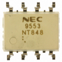
PS9553L3-E3-AX NEC, PS9553L3-E3-AX Datasheet

PS9553L3-E3-AX
Specifications of PS9553L3-E3-AX
Related parts for PS9553L3-E3-AX
PS9553L3-E3-AX Summary of contents
Page 1
... DIP IGBT GATE DRIVE PHOTOCOUPLER DESCRIPTION The PS9553, PS9553L1, PS9553L2 and PS9553L3 are optically coupled isolators containing a GaAlAs LED on the input side and a photo diode, a signal processing circuit and a power output transistor on the output side on one chip. The PS9553 Series is designed specifically for high common mode transient immunity (CMR) and high switching speed ...
Page 2
... Lead Bending Type (Gull-wing) For Surface Mount +0.5 9.25 –0. +0.4 1.01 –0.2 2.54 0.5±0.15 2 PS9553,PS9553L1,PS9553L2,PS9553L3 PS9553 5 4 7.62 +0.5 6.5 –0 15˚ PS9553L3 5 4 9.65 ±0.4 +0.5 6.5 –0.1 0.74±0.25 Preliminary Data Sheet PN10705EJ01V0DS ...
Page 3
... Lead Bending Type (Gull-wing) For Long Creepage Distance (Surface Mount) +0.5 9.25 –0. +0.4 1.01 –0.2 2.54 0.5±0.15 PS9553,PS9553L1,PS9553L2,PS9553L3 PS9553L1 5 10.16 4 +0.5 6.5 –0 15˚ PS9553L2 5 4 11.8 ±0.4 +0.5 6.5 –0.1 0.9±0.25 ...
Page 4
... OFF MARKING EXAMPLE No. 1 pin Mark 9553 NT831 Week Assembled Year Assembled (Last 1 Digit) In-house Code Rank Code PHOTOCOUPLER CONSTRUCTION Parameter PS9553, PS9553L3 Air Distance (MIN.) Outer Creepage Distance (MIN.) Isolation Distance (MIN.) 4 PS9553,PS9553L1,PS9553L2,PS9553L3 (Tr. 1) (Tr. 2) SHIELD Tr. 2 Output ON OFF H OFF ...
Page 5
... Pins 1-4 shorted together, 5-8 shorted together. μ ≤ 0.4 A (≤ (PEAK) OL (PEAK) RECOMMENDED OPERATING CONDITIONS Parameter Symbol Supply Voltage (V CC Forward Current (ON (ON) Forward Voltage (OFF (OFF) Operating Ambient Temperature PS9553,PS9553L1,PS9553L2,PS9553L3 = 25°C, unless otherwise specified) A Ratings Unit 1 0.6 A 0.6 ...
Page 6
... Threshold Input Voltage (H → L) Isolation Capacitance − Typical values 25° μ *2 Maximum pulse width = 50 s, Maximum duty cycle = 0.5%. μ *3 Maximum pulse width = 10 s, Maximum duty cycle = 0. measured with the DC load current in this testing PS9553,PS9553L1,PS9553L2,PS9553L3 = −40 to +100° Conditions mA 25° 25°C R ...
Page 7
... High Level Output Common Mode Transient Immunity at |CM *3 Low Level Output − Typical values 25° This load condition is equivalent to the IGBT load at 1 200 V/ Connect pin 1 and pin 4 to the LED common. PS9553,PS9553L1,PS9553L2,PS9553L3 = −40 to +100° Conditions mA, PLH Ω nF kHz, ...
Page 8
... TEST CIRCUIT Fig Test Circuit μ 0 SHIELD Fig Test Circuit μ 0 SHIELD Fig Test Circuit FLH 0 SHIELD 8 PS9553,PS9553L1,PS9553L2,PS9553L3 Fig SHIELD Fig 100 mA 4 SHIELD μ > Preliminary Data Sheet PN10705EJ01V0DS Test Circuit OL 8 μ Test Circuit μ 0 100 mA 5 ...
Page 9
... DUTY 4 5 CYCLE SHIELD Fig. 7 CMR Test Circuit and Wave Forms SHIELD Remark CMR Test : Connect pin 1 and pin 4 to the LED common. Preliminary Data Sheet PN10705EJ01V0DS PS9553,PS9553L1,PS9553L2,PS9553L3 , Test Circuit and Wave Forms PHL μ 0 Ω OUT t PLH V CM μ ...
Page 10
... TAPING SPECIFICATIONS (UNIT: mm) Outline and Dimensions (Tape) 2.0±0.1 4.0±0.1 2.05±0.05 Tape Direction Outline and Dimensions (Reel) R 1.0 Packing: 1 000 pcs/reel 10 PS9553,PS9553L1,PS9553L2,PS9553L3 +0.1 1.5 –0 10.7±0.1 12.0±0.1 PS9553L2-E3 2.0±0.5 13.0±0.2 21.0±0.8 Preliminary Data Sheet PN10705EJ01V0DS 4.5 MAX. 4.1 ± ...
Page 11
... PS9553,PS9553L1,PS9553L2,PS9553L3 Outline and Dimensions (Tape) 2.0±0.1 4.0±0.1 1.55±0.1 12.0±0.1 Tape Direction PS9553L3-E3 Outline and Dimensions (Reel) 2.0±0.5 13.0±0.2 R 1.0 Packing: 1 000 pcs/reel Preliminary Data Sheet PN10705EJ01V0DS +0.1 1.5 –0 5.3 MAX. 10.3±0.1 4.75±0.1 0.35± ...
Page 12
... RECOMMENDED MOUNT PAD DIMENSIONS (UNIT: mm) Part Number Lead Bending lead bending type (Gull-wing) PS9553L2 for long creepage distance (surface mount) lead bending type (Gull-wing) PS9553L3 for surface mount 12 PS9553,PS9553L1,PS9553L2,PS9553L3 10.2 2.54 8.2 2.54 Preliminary Data Sheet PN10705EJ01V0DS C D 1.7 2.2 1.7 ...
Page 13
... LED input. 3. Make sure the rise/fall time of the forward current is 0 order to avoid malfunctions, make sure the rise/fall slope of the supply voltage Avoid storage at a high temperature and high humidity. PS9553,PS9553L1,PS9553L2,PS9553L3 μ used between V and GND near device. Also, ensure that the CC μ ...
Page 14
... NEC Electronics' willingness to support a given application. (Note) (1) "NEC Electronics" as used in this statement means NEC Electronics Corporation and also includes its majority-owned subsidiaries. (2) "NEC Electronics products" means any product developed or manufactured by or for NEC Electronics (as defined above). 14 PS9553,PS9553L1,PS9553L2,PS9553L3 Preliminary Data Sheet PN10705EJ01V0DS Not all M8E 02. 11-1 ...
Page 15
... Exclude the product from general industrial waste and household garbage, and ensure that the product is controlled (as industrial waste subject to special control) up until final disposal. • Do not burn, destroy, cut, crush, or chemically dissolve the product. • Do not lick the product or in any way allow it to enter the mouth. PS9553,PS9553L1,PS9553L2,PS9553L3 ...


