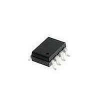
HCPL-2503#300 Avago Technologies US Inc., HCPL-2503#300 Datasheet - Page 9

HCPL-2503#300
Manufacturer Part Number
HCPL-2503#300
Description
OPTOCOUPLER 1MBS 8-SMD GW
Manufacturer
Avago Technologies US Inc.
Datasheet
1.HCPL-2503500.pdf
(12 pages)
Specifications of HCPL-2503#300
Input Type
DC
Package / Case
8-SMD Gull Wing
Voltage - Isolation
3750Vrms
Number Of Channels
1, Unidirectional
Current - Output / Channel
8mA
Data Rate
250kbps
Propagation Delay High - Low @ If
1µs @ 8mA
Current - Dc Forward (if)
25mA
Output Type
Open Collector
Mounting Type
Surface Mount, Gull Wing
Isolation Voltage
3750 Vrms
Output Device
Phototransistor
Configuration
1 Channel
Current Transfer Ratio
22 %
Maximum Baud Rate
1 MBps
Maximum Forward Diode Voltage
1.7 V
Maximum Reverse Diode Voltage
5 V
Maximum Input Diode Current
25 mA
Maximum Power Dissipation
100 mW
Maximum Operating Temperature
+ 70 C
Minimum Operating Temperature
0 C
Lead Free Status / RoHS Status
Contains lead / RoHS non-compliant
Available stocks
Company
Part Number
Manufacturer
Quantity
Price
9
Electrical Specifications
Over recommended temperature (T
Parameter
Logic High
Output Current
Logic High
Supply Current
Input Reverse
Breakdown Voltage
Input Capacitance
Input-Output
Insulation Leakage
Current
Resistance
(Input–Output)
Capacitance
(Input–Output)
*All typicals at 25˚C.
Notes:
5. Current Transfer Ratio is defined as the ratio of output collector current, I/O, to the forward LED input current, I
6. Device considered a two-terminal device: Pins 1, 2, 3, and 4 shorted together and Pins 5, 6, 7, and 8 shorted together.
7. Common mode transient immunity in Logic High level is the maximum tolerable (positive) dV
8. The 7.5 k load represents 1 LSTTL until load of 0.36 mA and a 20 kΩ pull-up resistor.
9. The 4.7 k load represents 1 LSTTL unit load of 0.36 mA and an 8.2 kΩ pull-up resistor.
pulse V
the maximum tolerable (negative) dV
in a Logic Low state (i.e., V
CM
, to assure that the output will remain in a Logic High state (i.e., V
O
< 0.8 V).
Symbol
I
I
V
C
I
R
C
OH
CCH
I–O
I–O
R
IN
I–O
CM
/dt on the trailing edge of the common mode pulse signal, V
A
= 0˚C to +70˚C) unless otherwise specified.
Min.
5
Typ.*
0.5
0.05
60
10
0.6
12
Max.
50
4
1.0
O
> 2.0 V). Common mode transient immunity in Logic Low level is
Units
nA
µA
µA
V
pF
µA
Ω
pF
Test Conditions
T
V
I
V
I
V
I
f = 1 MHz, V
45% Relative Humidity,
t = 5s, V
T
V
f = 1 MHz
F
F
F
A
A
O
O
O
I–O
= 0 mA
= 0 mA
= 10 µA, T
= 25°C, I
= 25°C
CM
= V
= V
= Open, V
= 500 Vdc
/dt on the leading edge of the common mode
CC
CC
I–O
= 5.5 V
CM
= 5.5 V
= 3000 Vdc,
, to assure that the output will remain
F
A
F
= 0 mA
= 0 V
= 25°C
CC
= 5.5 V
F
, times 100%.
Fig.
5
Note
6
6
6


