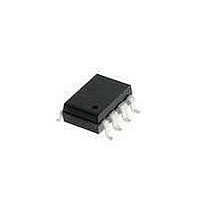
HCPL-3180-500 Avago Technologies US Inc., HCPL-3180-500 Datasheet

HCPL-3180-500
Specifications of HCPL-3180-500
Available stocks
Related parts for HCPL-3180-500
HCPL-3180-500 Summary of contents
Page 1
... HCPL-3180 2.5 Amp Output Current, High Speed, Gate Drive Optocoupler Data Sheet Lead (Pb) Free RoHS 6 fully compliant RoHS 6 fully compliant options available; -xxxE denotes a lead-free product Description This family of devices consists of a GaAsP LED. The LED is optically coupled to an integrated circuit with a power stage ...
Page 2
... To order, choose a part number from the part number column and combine with the desired option from the option column to form an order entry. Example 1: HCPL-3180-560E to order product of 300 mil DIP Gull Wing Surface Mount package in Tape and Reel packaging with IEC/EN/DIN EN 60747-5-2 Safety Approval in RoHS compliant. Example 2: HCPL-3180 to order product of 300 mil DIP package in tube packaging and non RoHS compliant ...
Page 3
... HCPL-3180 Gull Wing Surface Mount Option 300 9.65 ± 0.25 (0.380 ± 0.010 1.19 (0.047) MAX. 1.080 ± 0.320 (0.043 ± 0.013) 2.54 (0.100) BSC DIMENSIONS IN MILLIMETERS (INCHES). LEAD COPLANARITY = 0.10 mm (0.004 INCHES). NOTE: FLOATING LEAD PROTRUSION IS 0.25 mm (10 mils) MAX. Solder Reflow Temperature Profile 300 PREHEATING RATE 3°C + 1°C/–0.5°C/SEC. ...
Page 4
... Refer to the optocoupler section of the Isolation and Control Components Designer’s Catalog, under Product Safety Regulations section IEC/ EN/DIN EN 60747-5-2 for a detailed description of Method a and Method b partial discharge test profiles. ** Refer to the following figure for dependence Regulatory Information The HCPL-3180 has been approved by the following TIME WITHIN 5 °C of ACTUAL PEAK TEMPERATURE organizations: 20-40 SEC. ...
Page 5
... Peak Output Current “Low” Peak Output Current Supply Voltage Output Voltage Output Power Dissipation Total Power Dissipation Lead Solder Temperature Solder Reflow Temperature Profile 5 HCPL-3180 Units Conditions 7.1 mm Measured from input terminals to output terminals, shortest distance through air. 7.4 mm Measured from input terminals to output terminals, shortest distance path along body ...
Page 6
Recommended Operating Conditions Parameter Power Supply Input Current (ON) Input Voltage (OFF) Operating Temperature Electrical Specifications (DC) Over recommended operating conditions unless otherwise specified. Parameter Symbol High Level Output Current I OH Low Level Output Current I OL High Level Output Voltage V Low ...
Page 7
... PLH V signal. O 15. The difference between t and t between any two HCPL-3180 parts under same test conditions. PHL PLH 7 Min. Typ. Max. 50 150 ...
Page 8
-100 mA OUT -0 -1.0 -1.5 -2.0 -2.5 -3.0 -40 - 100 – ...
Page 9
PHL T = 25° PLH = 10 Ω 200 DUTY CYCLE = 50 250 kHz 150 100 ...
Page 10
Figure 17. I test circuit Figure 19. V test circuit 0.1 µ ...
Page 11
... OL realizes the very low V by using a DMOS transistor with (typical) on resistance in its pull down circuit. When the HCPL-3180 is in the low state, the IGBT gate is shorted + 1 W. Minimizing R to the emitter inductance from the HCPL-3180 to the IGBT gate and emitter (possibly by mounting HCPL-3180 on a small PC ...
Page 12
... V + 0.85 µ * 200 kHz O = 260 mW ≥ 226 mW (P O(MAX) The value of 4.5 mA for I in the previous equation was obtained by derating CC the I max max at +75°C. Since the must be increased to reduce the HCPL-3180 power dissipa- O(MAX) g tion – P O(SWITCHING MAX) O(MAX) = 226 mW – 136 SW(MAX) ...
Page 13
... CA ments using a 2.5 x 2.5 inch PC board, with small traces (no ground plane), a single HCPL- 3180 soldered into the center of the board and still air. The absolute maximum power dissipation derating specifications assume a q which CA value of +83 °C/W. From the thermal mode in Figure 27, ...
Page 14
... Without a detector shield, the dominant cause of op- tocoupler CMR failure is capacitive coupling from the input side of the optocoupler, through the package, to the detector IC as shown in Figure 28. The HCPL-3180 improves CMR performance by using a detector IC with an optically transparent Faraday shield, which diverts the capacitively coupled current away from the sensitive IC circuitry ...
Page 15
... HCPL- 3180 V threshold (typ 7.5 V) the optocoupler output UVLO- will go into the low state. When the HCPL-3180 output is in the low state and the supply voltage rises above the HCPL-3180 V threshold (typ 8.5 V) the optocoupler UVLO+ output will go into the high state (assume LED is “ ...
Page 16
... The maximum dead time is equivalent to the difference between the maximum and minimum propagation delay difference specification as shown in Figure 35. The maximum dead time for the HCPL-3180 is 180 ns-(- 90 ns)) over the operating temperature range of –40 °C to +100 °C. I ...


