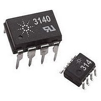
HCPL-3120-360E Avago Technologies US Inc., HCPL-3120-360E Datasheet - Page 20

HCPL-3120-360E
Manufacturer Part Number
HCPL-3120-360E
Description
OPTOCOUPLER 1CH 2.5A VDE 8SMD GW
Manufacturer
Avago Technologies US Inc.
Datasheet
1.HCPL-3120-500E.pdf
(24 pages)
Specifications of HCPL-3120-360E
Voltage - Isolation
3750Vrms
Number Of Channels
1, Unidirectional
Current - Output / Channel
2.5A
Propagation Delay High - Low @ If
300ns @ 7mA ~ 16mA
Current - Dc Forward (if)
25mA
Input Type
DC
Output Type
Gate Driver
Mounting Type
Surface Mount, Gull Wing
Package / Case
8-SMD Gull Wing
No. Of Channels
1
Optocoupler Output Type
Gate Drive
Input Current
16mA
Output Voltage
30V
Opto Case Style
SMD
No. Of Pins
8
Peak Reflow Compatible (260 C)
Yes
Isolation Voltage
3.75kV
Lead Free Status / RoHS Status
Lead free / RoHS Compliant
Available stocks
Company
Part Number
Manufacturer
Quantity
Price
Company:
Part Number:
HCPL-3120-360E
Manufacturer:
AVAGO
Quantity:
40 000
Part Number:
HCPL-3120-360E
Manufacturer:
AVAGO/安华高
Quantity:
20 000
Thermal Model (Discussion applies to HCPL-3120, HCPL-
J312 and HCNW3120)
The steady state thermal model for the HCPL-3120 is
shown in Figure 28. The thermal resistance values given
in this model can be used to calculate the temperatures
at each node for a given operating condition. As shown
by the model, all heat generated flows through q
raises the case temperature T
of q
and is, therefore, determined by the designer. The value
of q
ments using a 2.5 x 2.5 inch PC board, with small traces
(no ground plane), a single HCPL-3120 soldered into the
center of the board and still air. The absolute maximum
power dissipation derating specifications assume a
q
From the thermal mode in Figure 28 the LED and detector
IC junction temperatures can be expressed as:
T
q
+ P
q
q
T
q
+ P
Inserting the values for q
gives:
T
+ P
T
+ P
For example, given P
and q
T
= 45 mW
T
= 45 mW
T
board layout and part placement (q
plication.
20
JD
JE
JE
JD
JE
JD
JE
CA
= P
= P
and T
D
= P
D
=
= P
= P
value of 83°C/W.
CA
CA
•
•(——————— + q
P
E @
(q
depends on the conditions of the board design
E
E
= 83°C/W was obtained from thermal measure-
E
D
D
E
E
CA
(——————— + q
•
•
•
•
DC
•
•
•
LC
(q
140°C/W + 70°C = 120°C
= 83°C/W:
339°C/W + P
140°C/W + P
JD
(256°C/W + q
(57°C/W + q
(57°C/W + q
(111°C/W + q
+ q
||(q
LC
LC
should be limited to 125°C based on the
LC
•
•
||(q
+ q
LD
LC
140°C/W + 250 m
* q
339°C/W + 250 m
DC
LD
• q
+ q
+ q
DC
DC
+ q
DC
+ q
LC
LD
E
DC
) + q
D
D
CA
= 45 mW, P
CA
LD
•
CA
•
CA
) + q
) + T
)
140°C/W + T
194°C/W + T
)
LC
CA
) + T
and q
CA
) + T
CA
A
CA
W
A
) + T
)
W
C
A
•
)
accordingly. The value
194°C/W + 70°C = 125°C
O
DC
A
= 250 mW, T
CA
shown in Figure 28
A
A
) specific to the ap-
CA
A
= 70°C
which
P
I
V
Duty Cycle
P
I
V
V
E
f
Figure 27. Energy dissipated in the HCPL-3120 for each IGBT switching
cycle.
F
CC
E
O
SW
F
CC
EE
Parameter
Parameter
(Rg,Qg)
14
12
10
8
6
4
2
0
0
Rg – GATE RESISTANCE – Ω
10
HCPL-3120 fig 27
20
LED Current
LED On Voltage
Maximum LED Duty Cycle
Description
Description
Supply Current
Positive Supply Voltage
Negative Supply Voltage
Energy Dissipated in the HCPL-3120
for each IGBT Switching Cycle
(See Figure 27)
Switching Frequency
V
V
30
Qg = 100 nC
Qg = 500 nC
Qg = 1000 nC
CC
EE
= -9 V
= 19 V
40
50


