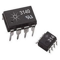
HCPL-3120-360E Avago Technologies US Inc., HCPL-3120-360E Datasheet - Page 23

HCPL-3120-360E
Manufacturer Part Number
HCPL-3120-360E
Description
OPTOCOUPLER 1CH 2.5A VDE 8SMD GW
Manufacturer
Avago Technologies US Inc.
Datasheet
1.HCPL-3120-500E.pdf
(24 pages)
Specifications of HCPL-3120-360E
Voltage - Isolation
3750Vrms
Number Of Channels
1, Unidirectional
Current - Output / Channel
2.5A
Propagation Delay High - Low @ If
300ns @ 7mA ~ 16mA
Current - Dc Forward (if)
25mA
Input Type
DC
Output Type
Gate Driver
Mounting Type
Surface Mount, Gull Wing
Package / Case
8-SMD Gull Wing
No. Of Channels
1
Optocoupler Output Type
Gate Drive
Input Current
16mA
Output Voltage
30V
Opto Case Style
SMD
No. Of Pins
8
Peak Reflow Compatible (260 C)
Yes
Isolation Voltage
3.75kV
Lead Free Status / RoHS Status
Lead free / RoHS Compliant
Available stocks
Company
Part Number
Manufacturer
Quantity
Price
Company:
Part Number:
HCPL-3120-360E
Manufacturer:
AVAGO
Quantity:
40 000
Part Number:
HCPL-3120-360E
Manufacturer:
AVAGO/安华高
Quantity:
20 000
Under Voltage Lockout Feature. (Discussion applies to
HCPL-3120, HCPL-J312, and HCNW3120)
The HCPL-3120 contains an under voltage lockout (UVLO)
feature that is designed to protect the IGBT under fault
conditions which cause the HCPL-3120 supply voltage
(equivalent to the fully-charged IGBT gate voltage) to
drop below a level necessary to keep the IGBT in a low re-
sistance state. When the HCPL-3120 output is in the high
state and the supply voltage drops below the HCPL-
3120 V
coupler output will go into the low state with a typical
delay, UVLO Turn Off Delay, of 0.6 µs.
When the HCPL-3120 output is in the low state and
the supply voltage rises above the HCPL-3120 V
threshold (11.0 < V
will go into the high state (assumes LED is “ON”) with a
typical delay, UVLO Turn On Delay of 0.8 µs.
Figure 36. Waveforms for dead time.
23
*PDD = PROPAGATION DELAY DIFFERENCE
NOTE: FOR DEAD TIME AND PDD CALCULATIONS ALL PROPAGATION
DELAYS ARE TAKEN AT THE SAME TEMPERATURE AND TEST CONDITIONS.
V
V
I
I
OUT1
OUT2
LED1
LED2
UVLO–
threshold (9.5 < V
(t
PHL-
PDD* MAX
Q1 ON
Q2 OFF
t
UVLO+
t
PHL MIN
PHL MAX
HCPL-3120 fig 36
t
PLH
)
MAX
< 13.5) the optocoupler output
MAXIMUM DEAD TIME
(DUE TO OPTOCOUPLER)
= (t
= (t
= PDD* MAX – PDD* MIN
PHL MAX
PHL MAX
t
MIN
PLH
t
PLH MAX
UVLO–
- t
- t
PHL MIN
PLH MIN
< 12.0) the opto-
) + (t
) – (t
Q1 OFF
PLH MAX
PHL MIN
Q2 ON
- t
- t
PLH MAX
PLH MIN
UVLO+
)
)
IPM Dead Time and Propagation Delay Specifications.
(Discussion applies to HCPL-3120, HCPL-J312, and
HCNW3120)
The HCPL-3120 includes a Propagation Delay Difference
(PDD) specification intended to help designers minimize
“dead time” in their power inverter designs. Dead time
is the time period during which both the high and low
side power transistors (Q1 and Q2 in Figure 25) are off.
Any overlap in Q1 and Q2 conduction will result in large
currents flowing through the power devices between
the high and low voltage motor rails.
Figure 35. Minimum LED skew for zero dead time.
V
V
I
I
OUT1
OUT2
LED1
LED2
*PDD = PROPAGATION DELAY DIFFERENCE
NOTE: FOR PDD CALCULATIONS THE PROPAGATION DELAYS
ARE TAKEN AT THE SAME TEMPERATURE AND TEST CONDITIONS.
HCPL-3120 fig 35
PDD* MAX = (t
t
PHL MAX
Q2 OFF
Q1 ON
t
PLH MIN
PHL
- t
PLH
)
MAX
= t
Q1 OFF
Q2 ON
PHL MAX
- t
PLH MIN


