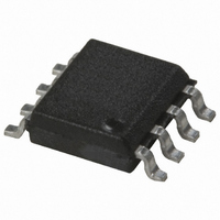
ACPL-072L-500E Avago Technologies US Inc., ACPL-072L-500E Datasheet - Page 8

ACPL-072L-500E
Manufacturer Part Number
ACPL-072L-500E
Description
OPTOCOUPLER 3.3/5V 25MBD 8-SOIC
Manufacturer
Avago Technologies US Inc.
Datasheet
1.ACPL-072L-000E.pdf
(11 pages)
Specifications of ACPL-072L-500E
Package / Case
8-SOIC (0.154", 3.90mm Width)
Voltage - Isolation
3750Vrms
Number Of Channels
1, Unidirectional
Current - Output / Channel
10mA
Data Rate
25MBd
Propagation Delay High - Low @ If
23.5ns
Input Type
Logic
Output Type
Push-Pull, Totem-Pole
Mounting Type
Surface Mount
Maximum Fall Time
8 ns
Maximum Rise Time
9 ns
Output Device
Logic Gate Photo IC
Configuration
1 Channel
Maximum Baud Rate
25 MBps
Maximum Power Dissipation
150 mW
Maximum Operating Temperature
+ 105 C
Minimum Operating Temperature
- 40 C
Number Of Elements
1
Baud Rate
25Mbps
Output Current
10mA
Isolation Voltage
3750Vrms
Package Type
SOIC
Operating Temp Range
-40C to 105C
Power Dissipation
150mW
Propagation Delay Time
40ns
Pin Count
8
Mounting
Surface Mount
Operating Temperature Classification
Industrial
Lead Free Status / RoHS Status
Lead free / RoHS Compliant
Lead Free Status / RoHS Status
Lead free / RoHS Compliant, Lead free / RoHS Compliant
Available stocks
Company
Part Number
Manufacturer
Quantity
Price
Company:
Part Number:
ACPL-072L-500E
Manufacturer:
AD
Quantity:
450
Company:
Part Number:
ACPL-072L-500E
Manufacturer:
AVAGO
Quantity:
15 000
Table 6. Switching Specifications
Test conditions that are not specified can be anywhere within the recommended operating range.
The following specifications cover the following power supply combinations: (4.5V≤V
(3V≤V
All typical specifications are at T
Table 7. Package Characteristics
All typical specifications are at T
Notes:
1. Absolute Maximum ambient operating temperature means the device will not be damaged if operated under these conditions. It does not
2. The LED is ON when V
3. t
4. The minimum pulse width is the shortest pulse width at which the specified pulse width distortion is guaranteed.
5. The maximum data rate is the fastest data rate at which the specified pulse width distortion is guaranteed.
6. PWD is defined as |t
7. t
8
Parameter
Propogation Delay Time
to Logic Low Output
Propogation Delay Time
to Logic High Output
Pulse Width
Maximum Data Rate
Pulse Width Distortion
| t
Propagation Delay Skew
Output Rise Time
(10% – 90%)
Output Fall Time
(90% - 10%)
Common Mode Transient
Immunity at Logic High Output
Common Mode Transient
Immunity at Logic Low Output
Parameters
Input-Output Momentary
With-stand Voltage
Input-Output Resistance
Input-Output Capacitance
Input Capacitance
Input IC Junction-to-Case
Thermal Resistance
Output IC Junction-to-Case
Thermal Resistance
Package Power Dissipation
PHL
guarantee functionality.
propagation delay is measured from the 50% level on the rising edge of the V
recommended operating conditions.
PHL
PSK
DD1
is equal to the magnitude of the worst case difference in t
- t
propagation delay is measured from the 50% level on the falling edge of the V
PLH
≤3.6V, 3V≤V
[4]
|
[12]
[7,8,9]
PHL
[5]
[3]
I
[3]
is low and OFF when V
[6]
DD2
- t
PLH
[7]
[9]
≤3.6V), (4.5V≤V
|. %PWD (percent pulse width distortion) is equal to the PWD divided by pulse width.
[8]
[8]
072L
772L
772L with
020 option
772L
072L
772L
072L
P
A
A
PD
=+25°C, V
= 25°C.
Symbol
t
t
t
t
t
t
| CM
| CM
|PWD |
PHL
PLH
PW
PSK
R
F
I
is high.
H
L
DD1
|
|
DD1
Symbol
V
R
C
C
qjci
qjco
≤5.5V, 3V≤V
ISO
I-O
I-O
I
Min.
40
10
10
= V
DD2
PHL
Min.
3750
3750
5000
= +3.3V.
and/or t
DD2
Typ.
23.5
25.5
2
9
8
20
20
≤3.6V) and (3V≤V
PLH
Typ.
10
0.6
3.0
145
160
140
135
12
I
that will be seen between units at any given temperature within the
signal to the 50% level of the rising edge of the V
Max.
40
40
25
6
20
I
signal to the 50% level of the falling edge of the V
Max.
150
Units
ns
ns
ns
MBd
ns
ns
ns
ns
kV/ms
kV/ms
DD1
Units
V rms
W
pF
pF
°C/W
°C/W
mW
≤3.6V, 4.5V≤V
Test Conditions
C
C
C
C
C
C
C
C
V
V
V
V
L
L
L
L
L
L
L
L
CM
I
CM
I
= V
= 0 V, V
= 15 pF, CMOS Signal Levels
= 15 pF, CMOS Signal Levels
= 15 pF, CMOS Signal Levels
= 15 pF, CMOS Signal Levels
= 15 pF, CMOS Signal Levels
= 15 pF, CMOS Signal Levels
= 15 pF, CMOS Signal Levels
= 15 pF, CMOS Signal Levels
Test Conditions
RH
V
f = 1 MHz
Thermocouple located at center
underside of package
= 1000 V, T
= 1000 V, T
DD1
I-O
≤
= 500 V dc
, V
O
50%, t = 1 min, T
DD1
O
< 0.8 V
≤5.5V, 4.5V≤V
> 0.8 V
DD2
A
A
= 25°C,
= 25°C,
≤5.5V).
DD1
O
A
signal.
= 25°C
DD2
O
signal. t
≤5.5V),
PLH


