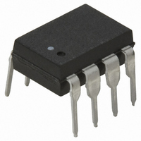
HCPL-2630 Avago Technologies US Inc., HCPL-2630 Datasheet

HCPL-2630
Specifications of HCPL-2630
Available stocks
Related parts for HCPL-2630
HCPL-2630 Summary of contents
Page 1
... PIN 7 IS NOT CONNECTED. A 0.1 F bypass capacitor must be connected between pins 5 and 8. H 6N135/6 HCNW135/6 HCNW4502/3 HCPL-0452/3 HCPL-0500/1 HCPL-4502/3 Description These diode-transistor optocoup- lers use an insulating layer between a LED and an integrated photodetector to provide elec- trical insulation between input and output. Separate connections ...
Page 2
... These single channel optocoup- lers are available in 8-Pin DIP, SO-8 and Widebody package configurations. The 6N135, HCPL-0500, and HCNW135 are for use in TTL/ CMOS, TTL/LSTTL or wide bandwidth analog applications. Current transfer ratio (CTR) for these devices is 7% minimum mA. F Selection Guide ...
Page 3
... Tape and Reel Packaging Option Option data sheets available. Contact your Hewlett-Packard sales representative or authorized distributor for information. *For 6N135/6 and HCPL-4502/3 only. **For HCPL-4503 only. Combination of Option 020 and Option 060 is not available. †Gull wing surface mount option applies to through hole parts only. Schematic I ...
Page 4
... TYPE NUMBER HP XXXXZ YYWW 1.19 (0.047) MAX. 1.080 ± 0.320 (0.043 ± 0.013) 8-Pin DIP Package with Gull Wing Surface Mount Option 300 (6N135/6, HCPL-4502/3) 9.65 ± 0.25 (0.380 ± 0.010 1.19 (0.047) MAX. 1.080 ± 0.320 (0.043 ± 0.013) 2 ...
Page 5
... Small Outline SO-8 Package (HCPL-0500/1, HCPL-0452/ 3.937 ± 0.127 (0.155 ± 0.005 0.381 ± 0.076 (0.016 ± 0.003) 5.080 ± 0.127 (0.200 ± 0.005) 3.175 ± 0.127 (0.125 ± 0.005) DIMENSIONS IN MILLIMETERS (INCHES). LEAD COPLANARITY = 0.10 mm (0.004 INCHES). 8-Pin Widebody DIP Package (HCNW135/6, HCNW4502/3) 11.15 ± ...
Page 6
... BSC DIMENSIONS IN MILLIMETERS (INCHES). LEAD COPLANARITY = 0.10 mm (0.004 INCHES). Solder Reflow Temperature Profile (HCPL-0500/1, HCPL-0452/3, and Gull Wing Surface Mount Option Parts) 260 240 220 T = 115°C, 0.3°C/SEC 200 180 160 ...
Page 7
Regulatory Information The devices contained in this data sheet have been approved by the following organizations: UL Recognized under UL 1577, Component Recognition Program, File E55361. Insulation and Safety Related Specifications Parameter Symbol Minimum External L(101) Air Gap (External Clearance) ...
Page 8
... VDE 0884 Insulation Related Characteristics (HCPL-4503 OPTION 060 ONLY) Description Installation classification per DIN VDE 0110/1.89, Table 1 for rated mains voltage 300 V rms for rated mains voltage 450 V rms Climatic Classification Pollution Degree (DIN VDE 0110/1.89) Maximum Working Insulation Voltage Input to Output Test Voltage, Method ...
Page 9
Absolute Maximum Ratings Parameter Storage Temperature* Operating Temperature* Average Forward Input Current* Peak Forward Input Current* (50% duty cycle pulse width) (50% duty cycle pulse width) Peak Transient Input Current pulse width, 300 ...
Page 10
... CTR* 6N135 Transfer Ratio HCPL-0500 HCNW135 6N136 HCPL-4502/3 HCPL-0501 HCPL-0452/3 HCNW136 HCNW4502/3 Logic Low V 6N135 OL Output Voltage HCPL-0500 HCNW135 6N136 HCPL-4502/3 HCPL-0501 HCPL-0452/3 HCNW136 HCNW4502/3 Logic High Output Current Logic Low I CCL Supply Current Logic High I * CCH Supply Current Input Forward ...
Page 11
... Level Output HCPL-4502 HCPL-0501 HCPL-0452 HCNW4502 HCPL-4503 HCPL-0453 HCNW4503 Common Mode |CM | 6N135 L HCPL-0500 Transient HCNW135 Immunity at Logic Low 6N136 Level Output HCPL-4502 HCPL-0501 HCPL-0452 HCNW4502 HCPL-4503 HCPL-0453 HCNW4503 Bandwidth BW 6N135/6 HCPL-0500/1 HCNW135/6 *For JEDEC registered parts. **All typicals 1- C unless otherwise specified. ...
Page 12
Package Characteristics Over recommended temperature (T Parameter Sym. Device Input-Output V 8-Pin DIP ISO Momentary SO-8 Withstand Widebody Voltage** 8-Pin DIP (Option 020) I 8-Pin DIP I-O Input-Output R 8-Pin DIP I-O Resistance SO-8 Widebody Input-Output C 8-Pin DIP I-O ...
Page 13
... T = 25° 5 – OUTPUT VOLTAGE – Figure 1. DC and Pulsed Transfer Characteristics. 8 PIN DIP, SO-8 1.5 6N135, HCPL-0500 6N136, HCPL-4502/3 HCPL-0501/0452/0453 1.0 0.5 NORMALIZED 0 25° 100 I – INPUT CURRENT – Figure 2. Current Transfer Ratio vs. Input Current. 8 PIN DIP, SO-8 ...
Page 14
... HCPL-0501, 0452, 0453 0.6 -60 -40 - 100 T – TEMPERATURE – °C A Figure 4. Current Transfer Ratio vs. Temperature. 8 PIN DIP, SO-8 2000 mA 5 6N135, HCPL-0500 ( 6N136, HCPL-0501 HCPL-4502 1 1500 HCPL-0452/3 1000 t t PHL PLH 500 0 -60 - 100 T – TEMPERATURE – Figure 5. Propagation Delay vs. Temperature. ...
Page 15
... Figure 7. Logic High Output Current vs. Temperature. 8 PIN DIP, SO-8 0. 25° 100 , 0.20 0. – QUIESCENT INPUT CURRENT – Figure 8. Small-Signal Current Transfer Ratio vs. Quiescent Input Current. HCPL-4503 OPTION 060 800 P (mW) S 700 I (mA) S 600 500 400 300 200 100 100 125 150 175 200 T – ...
Page 16
... HCPL-0500 ° -10 -15 -20 0.1 1.0 10 100 f - FREQUENCY - MHz HCNW135/6 Figure 10. Frequency Response. 6N135/6, HCPL-0500/1 + 0.1 µF 2 µF 3 100 TRIM FOR UNITY GAIN 22 1N4150 HCNW135 0.1 µF 470 ( TEST INPUT) 5 100 2N3904 TYPICAL LINEARITY = ± p-p IN TYPICAL SNR = 50dB TYPICAL R = 375 ...
Page 17
... V O 1 PHL PLH Figure 11. Switching Test Circuit 90% 90% 10% 10 SWITCH SWITCH *PIN 7 UNCONNECTED IN HCPL-4502/3, HCPL-0542/3, HCNW4502/3 Figure 12. Test Circuit for Transient Immunity and Typical Waveforms. 1-32 I PULSE GEN 10% DUTY CYCLE 1/f < 100 µ MONITOR PIN 7 UNCONNECTED IN HCPL-4502/3, HCPL-0452/3, HCNW4502 ...
Page 18
This datasheet has been download from: www.datasheetcatalog.com Datasheets for electronics components. ...


