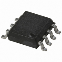
ACSL-6210-50R Avago Technologies US Inc., ACSL-6210-50R Datasheet

ACSL-6210-50R
Specifications of ACSL-6210-50R
Related parts for ACSL-6210-50R
ACSL-6210-50R Summary of contents
Page 1
... RoHS 6 fully compliant options available; -xxxE denotes a lead-free product Description ACSL-6xx0 are truly isolated, multi-channel and bi-direc- tional, high-speed optocouplers. Integration of multiple optocouplers in monolithic form is achieved through patented process technology. These devices provide full duplex and bi-directional isolated data transfer and communication capability in compact surface mount packages ...
Page 2
... To order, choose a part number from the part number column and combine with the desired option from the option column to form an order entry. Example 1: ACSL-6210-56RE refers to ordering a Surface Mount SO-8 package in Tape and Reel packaging with IEC/EN/DIN EN 60747-5-2 Safety Approval in RoHS compliant. Example 2: ACSL-6400-00TE refers to ordering a Surface Mount SO-16 package product in tube packaging and in RoHS compliant ...
Page 3
... Functional Diagrams ACSL-6210 - Dual-Ch, Bi-Dir ACSL-6310 - Triple-Ch, Bi-Dir (2/1) ACSL-6410 - Quad-Ch, Bi-Dir (3/1) 3 ACSL-6300 - Triple-Ch, All-in-One ACSL-6400 - Quad-Ch, All-in-One ACSL-6420 - Quad-Ch, Bi-Dir (2/2) ...
Page 4
... Schematic Diagrams The ACSL-6xx0 series optocouplers feature the GaAsP LEDs with proprietary back emission design. They offer the designer a broad range of input drive current, from mA, thus providing greater flexibility in designing the drive circuit. The output detector integrated circuit (IC) in the opto- coupler consists of a photodiode at the input of a two- stage amplifi ...
Page 5
... ANODE3 6 CATHODE3 Shield 7 ANODE4 8 CATHODE4 Shield ACSL-6420 - Quad-Ch, Bi-Dir (2/2) Shield 1 GND1 2 Vo4 Shield 3 Vo3 4 VDD1 5 ANODE1 6 CATHODE1 Shield 7 ANODE2 8 CATHODE2 Shield 5 ACSL-6410 - Quad-Ch, Bi-Dir (3/1) 16 GND 1 GND1 15 CATHODE1 VDD 14 Vo1 2 Vo4 3 VDD1 13 Vo2 4 ANODE1 5 CATHODE2 12 Vo3 6 ANODE2 7 CATHODE3 11 Vo4 8 ANODE3 10 ...
Page 6
... DIMENSIONS: INCHES (MILLIMETERS) ACSL-6300, ACSL-6310, ACSL-6400, ACSL-6410 and ACSL-6420 Small Outline SO-16 Package 0.386 (9.802) 0.394 (9.999) 8 0.228 (5.791) 0.244 (6.197) 0.013 (0.330) 0.020 (0.508) 0.050 (1.270) 0.060 (1.524) ...
Page 7
Solder Reflow Temperature Profile 300 PREHEATING RATE 3 ° ° C/–0.5 ° C/SEC. REFLOW HEATING RATE 2.5 ° C ± 0.5 ° C/SEC. 200 160 ° C 150 ° C ° 140 C 100 ROOM TEMPERATURE 0 ...
Page 8
... Volts DIN IEC 112/VDE0303 Part 1 IIIa Material Group (DIN VDE 0110, 1/89, Table 1) Symbol V IORM IOTM S,INPUT P S,OUTPUT R IO 200 ACSL-6XX0-X6X Units I-IV I-III 55/100/21 2 560 V peak 1050 V peak 840 V peak 4000 V peak 175 °C 150 mA 600 Ω ...
Page 9
Absolute Maximum Ratings Parameter Storage Temperature Operating Temperature Supply Voltage (1 Minute Maximum) Reverse Input Voltage (Per Channel) Output Voltage (Per Channel) [1] Average Forward Input Current (Per Channel) Output Current (Per Channel) [2] Input Power Dissipation (Per Channel) Output ...
Page 10
Electrical Specifications Over recommended operating range (3.0V ≤ V All typical specifications are +25° Parameter Input Threshold Current High Level Output Current Low Level Output Voltage High Level Supply Current (per channel) Low Level ...
Page 11
Electrical Specifications Over recommended operating range (4.5V ≤ V All typical specifications are +25° Parameter Input Threshold Current High Level Output Current Low Level Output Voltage High Level Supply Current (per channel) Low Level Supply ...
Page 12
Package Characteristics All specifications are at T =+25°C. A Parameter Input-Output Momentary SO8 Withstand Voltage [9] SO16 Input-Output Insulation [10] [11] SO8 SO16 [10] Input-Output Resistance SO8 SO16 [10] Input-Output Capacitance SO8 SO16 Input-Input Insulation SO8 [12] Leakage Current SO16 ...
Page 13
Typical Performance 3. 0. 350Ω KΩ KΩ -60 -40 - 100 ...
Page 14
Typical Performance, continued 5. DDL DDH -60 -40 - ...
Page 15
... PULSE GEN 50Ω 5ns I F INPUT PHL 90% OUTPUT Figure 16. Test circuit for and t . PHL PLH F, R ACSL-6400 PULSE GEN Vcm 0 V SWITCH AT POSITION "A" (min.) SWITCH AT POSITION "B" 0.5 V Figure 17. Test circuit for common mode transient immunity and typical waveforms ...
Page 16
... Suggested Input Circuits for Driving the LED Figures 18, 19, and 20 show some of the several techniques for driving the ACSL-6xx0 LED. Figure 18 shows the rec- ommended circuit when using any type of TTL gate. The buffer PNP transistor allows the circuit to be used with TTL or CMOS gates that have low sinking current capabil- ity ...
Page 17
... HIGH when the LED is ON. If there is a design that requires the optocoupler to behave as a non-inverting gate, then Figure 19. CMOS drive circuit for the ACSL-6xx0. Figure 20. High CMR drive circuit for the ACSL-6xx0. 17 the series input drive circuit shown in Figure 19 can be used. This input drive circuit has an inverting function, and since the optocoupler also behaves as an inverter, the total circuit is non-inverting ...
Page 18
Propagation Delay, Pulse-Width Distortion and Propagation Delay Skew Propagation delay is a figure of merit which describes how quickly a logic signal propagates through a system. The propaga- tion delay from low to high ( the amount of ...
Page 19
For product information and a complete list of distributors, please go to our web site: Avago, Avago Technologies, and the A logo are trademarks of Avago Technologies in the United States and other countries. Data subject to change. Copyright © ...


