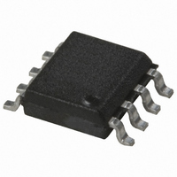
ACSL-6210-50R Avago Technologies US Inc., ACSL-6210-50R Datasheet - Page 16

ACSL-6210-50R
Manufacturer Part Number
ACSL-6210-50R
Description
OPTOCOUPLER DUAL BIDIR 8-SOIC
Manufacturer
Avago Technologies US Inc.
Datasheet
1.ACSL-6210-00RE.pdf
(19 pages)
Specifications of ACSL-6210-50R
Package / Case
8-SOIC (0.154", 3.90mm Width)
Voltage - Isolation
2500Vrms
Number Of Channels
2, Bi-Directional
Current - Output / Channel
50mA
Data Rate
15MBd
Propagation Delay High - Low @ If
44ns @ 8mA
Current - Dc Forward (if)
15mA
Input Type
DC
Output Type
Open Collector
Mounting Type
Surface Mount
Isolation Voltage
2500 Vrms
Maximum Continuous Output Current
50 mA
Maximum Fall Time
12 ns
Maximum Forward Diode Current
15 mA
Maximum Rise Time
35 ns
Minimum Forward Diode Voltage
1.25 V
Output Device
Logic Gate Photo IC
Configuration
2 Channel
Maximum Baud Rate
15 MBps
Maximum Forward Diode Voltage
1.8 V
Maximum Reverse Diode Voltage
5 V
Maximum Power Dissipation
60 mW
Maximum Operating Temperature
+ 100 C
Minimum Operating Temperature
- 40 C
Lead Free Status / RoHS Status
Contains lead / RoHS non-compliant
Application Information
ON and OFF Conditions
The ACSL-6xx0 series has the ON condition defined by
current, and the OFF condition defined by voltage. In order
to guarantee that the optocoupler is OFF, the forward
voltage across the LED must be less than or equal to
0.8 volt for the entire operating temperature range. This
has direct implications for the input drive circuit. If the
design uses a TTL gate to drive the input LED, then one has
to ensure that the gate output voltage is sufficient to cause
the forward voltage to be less than 0.8 volt. The typical
threshold current for the ACSL-6xx0 series optocouplers is
2.7 mA; however, this threshold could increase over time
due to the aging effects of the LED. Drive circuit arrange-
ments must provide for the ON state LED forward current
of at least 7 mA, or more if faster operation is desired.
Maximum Input Current and Reverse Voltage
The average forward input current should not exceed
the 15 mA Absolute Maximum Rating as stated; however,
peaking circuits with transient input currents up to 50 mA
are allowed provided the average current does not exceed
15 mA. If the input current maximum rating is exceeded,
Figure 18. TTL interface circuit for the ACSL-6xx0.
16
the local temperature of the LED can rise, which in turn may
affect the long-term reliability of the device. When designing
the input circuit, one must also ensure that the input reverse
voltage does not exceed 5 V. If the optocoupler is subjected
to reverse voltage transients or accidental situations that
may cause a reverse voltage to be applied, thus an anti-
parallel diode across the LED is recommended.
Suggested Input Circuits for
Driving the LED
Figures 18, 19, and 20 show some of the several techniques
for driving the ACSL-6xx0 LED. Figure 18 shows the rec-
ommended circuit when using any type of TTL gate. The
buffer PNP transistor allows the circuit to be used with
TTL or CMOS gates that have low sinking current capabil-
ity. One advantage of this circuit is that there is very little
variation in power supply current due to the switching of
the optocoupler LED. This can be important in high-reso-
lution analog-to-digital (A/D) systems where ground loop
currents due to the switching of the LEDs can cause distor-
tion in the A/D output.


