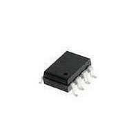
HCPL-3100-500E Avago Technologies US Inc., HCPL-3100-500E Datasheet - Page 5

HCPL-3100-500E
Manufacturer Part Number
HCPL-3100-500E
Description
OPTOCOUPLER GATE DRIVER 8-SMD
Manufacturer
Avago Technologies US Inc.
Datasheet
1.HCPL-3100.pdf
(14 pages)
Specifications of HCPL-3100-500E
Package / Case
8-SMD Gull Wing
Voltage - Isolation
5000Vrms
Number Of Channels
1, Unidirectional
Current - Output / Channel
100mA
Propagation Delay High - Low @ If
2µs @ 10mA
Current - Dc Forward (if)
20mA
Input Type
DC
Output Type
Push-Pull, Totem-Pole
Mounting Type
Surface Mount, Gull Wing
Isolation Voltage
5000 Vrms
Maximum Continuous Output Current
100 mA
Maximum Fall Time
0.5 us
Maximum Forward Diode Current
25 mA
Maximum Rise Time
0.5 us
Output Device
Integrated Photo IC
Configuration
1 Channel
Maximum Forward Diode Voltage
1.4 V
Maximum Reverse Diode Voltage
6 V
Maximum Power Dissipation
550 mW
Maximum Operating Temperature
+ 70 C
Minimum Operating Temperature
- 40 C
Number Of Elements
1
Forward Voltage
1.4V
Forward Current
25mA
Output Current
100mA
Package Type
PDIP SMD
Operating Temp Range
-40C to 100C
Fall Time
500ns
Rise Time
500ns
Power Dissipation
550mW
Propagation Delay Time
2000ns
Pin Count
8
Mounting
Surface Mount
Reverse Breakdown Voltage
6V
Operating Temperature Classification
Industrial
Lead Free Status / RoHS Status
Lead free / RoHS Compliant
Lead Free Status / RoHS Status
Lead free / RoHS Compliant, Lead free / RoHS Compliant
CONTROL
Recommended Operating Conditions
Power Supply Voltage
Input Current (ON)
Operating Temperature
INPUT
5
Recommended Protection for
Output Transistors
During switching transitions, the
output transistors Q1 and Q2 of
the HCPL-3100/3101 can
conduct large amounts of
current. Figure 1 describes a
Figure 1. Recommended output transistor protection and typical application circuit.
+5 V
TTL
OR
LSTTL
Parameter
TOTEM
POLE
OUTPUT
GATE
CATHODE
R
ANODE
3
R = 25 - 100
R = 180
BYPASS CAPACITOR C = 0.1 F
2
3
240
Symbol
(HCPL-3100)
(HCPL-3101)
HCPL-3100/1
V
T
I
CC
F
A
recommended circuit design
showing a current limiting
resistor R
order to prevent damage to the
output transistors Q1 and Q2.
(See Note 7.) A bypass capacitor
C
reduce power supply noise.
1
1
is also recommended to
Q1
Q2
HCPL-3100
HCPL-3101
2
Device
which is necessary in
8
7
6
5
R
2
C
1
12 V
Min.
-40
15
14
15
12 V
IGBT
(OR )t
(MOSFET)
Max.
30
20
20
70
Units
mA
mA
V
C
+ HVDC
- HVDC
3-PHASE
AC


